WO2012013707A1 - Heating arrangement and method for heating substrates - Google Patents
Heating arrangement and method for heating substrates Download PDFInfo
- Publication number
- WO2012013707A1 WO2012013707A1 PCT/EP2011/062912 EP2011062912W WO2012013707A1 WO 2012013707 A1 WO2012013707 A1 WO 2012013707A1 EP 2011062912 W EP2011062912 W EP 2011062912W WO 2012013707 A1 WO2012013707 A1 WO 2012013707A1
- Authority
- WO
- WIPO (PCT)
- Prior art keywords
- substrate
- heating
- enclosure
- plane
- processing system
- Prior art date
Links
- 238000010438 heat treatment Methods 0.000 title claims abstract description 186
- 239000000758 substrate Substances 0.000 title claims abstract description 149
- 238000000034 method Methods 0.000 title claims description 37
- 238000012545 processing Methods 0.000 claims abstract description 52
- 230000001678 irradiating effect Effects 0.000 claims abstract description 3
- 238000001816 cooling Methods 0.000 claims description 23
- OKTJSMMVPCPJKN-UHFFFAOYSA-N Carbon Chemical compound [C] OKTJSMMVPCPJKN-UHFFFAOYSA-N 0.000 claims description 21
- 239000000463 material Substances 0.000 claims description 20
- 238000000576 coating method Methods 0.000 claims description 18
- 239000011248 coating agent Substances 0.000 claims description 16
- 229910052799 carbon Inorganic materials 0.000 claims description 12
- PXHVJJICTQNCMI-UHFFFAOYSA-N Nickel Chemical compound [Ni] PXHVJJICTQNCMI-UHFFFAOYSA-N 0.000 claims description 10
- 229910002804 graphite Inorganic materials 0.000 claims description 9
- 239000010439 graphite Substances 0.000 claims description 9
- 239000000835 fiber Substances 0.000 claims description 8
- 229910052782 aluminium Inorganic materials 0.000 claims description 7
- XAGFODPZIPBFFR-UHFFFAOYSA-N aluminium Chemical compound [Al] XAGFODPZIPBFFR-UHFFFAOYSA-N 0.000 claims description 7
- RYGMFSIKBFXOCR-UHFFFAOYSA-N Copper Chemical compound [Cu] RYGMFSIKBFXOCR-UHFFFAOYSA-N 0.000 claims description 6
- BQCADISMDOOEFD-UHFFFAOYSA-N Silver Chemical compound [Ag] BQCADISMDOOEFD-UHFFFAOYSA-N 0.000 claims description 6
- 229910052802 copper Inorganic materials 0.000 claims description 6
- 239000010949 copper Substances 0.000 claims description 6
- PCHJSUWPFVWCPO-UHFFFAOYSA-N gold Chemical compound [Au] PCHJSUWPFVWCPO-UHFFFAOYSA-N 0.000 claims description 6
- 239000010931 gold Substances 0.000 claims description 6
- 229910052737 gold Inorganic materials 0.000 claims description 6
- 229910052709 silver Inorganic materials 0.000 claims description 6
- 239000004332 silver Substances 0.000 claims description 6
- 229910052759 nickel Inorganic materials 0.000 claims description 5
- 229920000049 Carbon (fiber) Polymers 0.000 claims description 4
- 239000004917 carbon fiber Substances 0.000 claims description 4
- 239000002131 composite material Substances 0.000 claims description 4
- 239000011819 refractory material Substances 0.000 claims description 4
- 230000003746 surface roughness Effects 0.000 claims description 3
- VNWKTOKETHGBQD-UHFFFAOYSA-N methane Chemical compound C VNWKTOKETHGBQD-UHFFFAOYSA-N 0.000 claims description 2
- HBMJWWWQQXIZIP-UHFFFAOYSA-N silicon carbide Chemical compound [Si+]#[C-] HBMJWWWQQXIZIP-UHFFFAOYSA-N 0.000 claims description 2
- 230000008569 process Effects 0.000 description 28
- 239000010409 thin film Substances 0.000 description 11
- 238000004519 manufacturing process Methods 0.000 description 10
- 230000000694 effects Effects 0.000 description 9
- 230000005855 radiation Effects 0.000 description 9
- 238000009826 distribution Methods 0.000 description 7
- 238000006243 chemical reaction Methods 0.000 description 6
- 230000003247 decreasing effect Effects 0.000 description 6
- 238000010521 absorption reaction Methods 0.000 description 5
- 230000003647 oxidation Effects 0.000 description 5
- 238000007254 oxidation reaction Methods 0.000 description 5
- QVGXLLKOCUKJST-UHFFFAOYSA-N atomic oxygen Chemical compound [O] QVGXLLKOCUKJST-UHFFFAOYSA-N 0.000 description 4
- 125000004122 cyclic group Chemical group 0.000 description 4
- 239000011521 glass Substances 0.000 description 4
- 229910052760 oxygen Inorganic materials 0.000 description 4
- 239000001301 oxygen Substances 0.000 description 4
- VYPSYNLAJGMNEJ-UHFFFAOYSA-N silicon dioxide Inorganic materials O=[Si]=O VYPSYNLAJGMNEJ-UHFFFAOYSA-N 0.000 description 4
- XLYOFNOQVPJJNP-UHFFFAOYSA-N water Substances O XLYOFNOQVPJJNP-UHFFFAOYSA-N 0.000 description 4
- 239000012809 cooling fluid Substances 0.000 description 3
- 230000007423 decrease Effects 0.000 description 3
- 238000000151 deposition Methods 0.000 description 3
- 230000008021 deposition Effects 0.000 description 3
- 238000005516 engineering process Methods 0.000 description 3
- 238000004518 low pressure chemical vapour deposition Methods 0.000 description 3
- 238000000623 plasma-assisted chemical vapour deposition Methods 0.000 description 3
- 239000002243 precursor Substances 0.000 description 3
- 239000010453 quartz Substances 0.000 description 3
- 239000000376 reactant Substances 0.000 description 3
- 239000003575 carbonaceous material Substances 0.000 description 2
- 238000013461 design Methods 0.000 description 2
- HQWPLXHWEZZGKY-UHFFFAOYSA-N diethylzinc Chemical compound CC[Zn]CC HQWPLXHWEZZGKY-UHFFFAOYSA-N 0.000 description 2
- 238000005265 energy consumption Methods 0.000 description 2
- 239000010408 film Substances 0.000 description 2
- 238000001914 filtration Methods 0.000 description 2
- 239000007788 liquid Substances 0.000 description 2
- 230000007246 mechanism Effects 0.000 description 2
- 238000005457 optimization Methods 0.000 description 2
- 238000005240 physical vapour deposition Methods 0.000 description 2
- 239000004065 semiconductor Substances 0.000 description 2
- WFKWXMTUELFFGS-UHFFFAOYSA-N tungsten Chemical compound [W] WFKWXMTUELFFGS-UHFFFAOYSA-N 0.000 description 2
- 229910052721 tungsten Inorganic materials 0.000 description 2
- 239000010937 tungsten Substances 0.000 description 2
- 238000000429 assembly Methods 0.000 description 1
- 230000000712 assembly Effects 0.000 description 1
- 238000001505 atmospheric-pressure chemical vapour deposition Methods 0.000 description 1
- 230000009286 beneficial effect Effects 0.000 description 1
- 238000005229 chemical vapour deposition Methods 0.000 description 1
- 230000002860 competitive effect Effects 0.000 description 1
- 230000008602 contraction Effects 0.000 description 1
- 229910021419 crystalline silicon Inorganic materials 0.000 description 1
- 230000001419 dependent effect Effects 0.000 description 1
- 239000000796 flavoring agent Substances 0.000 description 1
- 235000019634 flavors Nutrition 0.000 description 1
- 239000005329 float glass Substances 0.000 description 1
- 239000002241 glass-ceramic Substances 0.000 description 1
- 230000006872 improvement Effects 0.000 description 1
- 229910052751 metal Inorganic materials 0.000 description 1
- 239000002184 metal Substances 0.000 description 1
- 238000002488 metal-organic chemical vapour deposition Methods 0.000 description 1
- 150000002739 metals Chemical class 0.000 description 1
- 239000003921 oil Substances 0.000 description 1
- 230000001590 oxidative effect Effects 0.000 description 1
- 229910021420 polycrystalline silicon Inorganic materials 0.000 description 1
- 230000001681 protective effect Effects 0.000 description 1
- 238000002310 reflectometry Methods 0.000 description 1
- 238000001228 spectrum Methods 0.000 description 1
- 238000003860 storage Methods 0.000 description 1
- 239000000126 substance Substances 0.000 description 1
- 238000012546 transfer Methods 0.000 description 1
- 230000001131 transforming effect Effects 0.000 description 1
- 238000009489 vacuum treatment Methods 0.000 description 1
- 238000013022 venting Methods 0.000 description 1
Images


Classifications
-
- H—ELECTRICITY
- H01—ELECTRIC ELEMENTS
- H01L—SEMICONDUCTOR DEVICES NOT COVERED BY CLASS H10
- H01L21/00—Processes or apparatus adapted for the manufacture or treatment of semiconductor or solid state devices or of parts thereof
- H01L21/67—Apparatus specially adapted for handling semiconductor or electric solid state devices during manufacture or treatment thereof; Apparatus specially adapted for handling wafers during manufacture or treatment of semiconductor or electric solid state devices or components ; Apparatus not specifically provided for elsewhere
- H01L21/67005—Apparatus not specifically provided for elsewhere
- H01L21/67011—Apparatus for manufacture or treatment
- H01L21/67098—Apparatus for thermal treatment
- H01L21/67115—Apparatus for thermal treatment mainly by radiation
-
- H—ELECTRICITY
- H01—ELECTRIC ELEMENTS
- H01L—SEMICONDUCTOR DEVICES NOT COVERED BY CLASS H10
- H01L31/00—Semiconductor devices sensitive to infrared radiation, light, electromagnetic radiation of shorter wavelength or corpuscular radiation and specially adapted either for the conversion of the energy of such radiation into electrical energy or for the control of electrical energy by such radiation; Processes or apparatus specially adapted for the manufacture or treatment thereof or of parts thereof; Details thereof
- H01L31/18—Processes or apparatus specially adapted for the manufacture or treatment of these devices or of parts thereof
- H01L31/186—Particular post-treatment for the devices, e.g. annealing, impurity gettering, short-circuit elimination, recrystallisation
-
- H—ELECTRICITY
- H01—ELECTRIC ELEMENTS
- H01L—SEMICONDUCTOR DEVICES NOT COVERED BY CLASS H10
- H01L21/00—Processes or apparatus adapted for the manufacture or treatment of semiconductor or solid state devices or of parts thereof
- H01L21/67—Apparatus specially adapted for handling semiconductor or electric solid state devices during manufacture or treatment thereof; Apparatus specially adapted for handling wafers during manufacture or treatment of semiconductor or electric solid state devices or components ; Apparatus not specifically provided for elsewhere
- H01L21/67005—Apparatus not specifically provided for elsewhere
- H01L21/67011—Apparatus for manufacture or treatment
- H01L21/67098—Apparatus for thermal treatment
- H01L21/67109—Apparatus for thermal treatment mainly by convection
-
- H—ELECTRICITY
- H01—ELECTRIC ELEMENTS
- H01L—SEMICONDUCTOR DEVICES NOT COVERED BY CLASS H10
- H01L31/00—Semiconductor devices sensitive to infrared radiation, light, electromagnetic radiation of shorter wavelength or corpuscular radiation and specially adapted either for the conversion of the energy of such radiation into electrical energy or for the control of electrical energy by such radiation; Processes or apparatus specially adapted for the manufacture or treatment thereof or of parts thereof; Details thereof
- H01L31/04—Semiconductor devices sensitive to infrared radiation, light, electromagnetic radiation of shorter wavelength or corpuscular radiation and specially adapted either for the conversion of the energy of such radiation into electrical energy or for the control of electrical energy by such radiation; Processes or apparatus specially adapted for the manufacture or treatment thereof or of parts thereof; Details thereof adapted as photovoltaic [PV] conversion devices
- H01L31/052—Cooling means directly associated or integrated with the PV cell, e.g. integrated Peltier elements for active cooling or heat sinks directly associated with the PV cells
- H01L31/0521—Cooling means directly associated or integrated with the PV cell, e.g. integrated Peltier elements for active cooling or heat sinks directly associated with the PV cells using a gaseous or a liquid coolant, e.g. air flow ventilation, water circulation
-
- Y—GENERAL TAGGING OF NEW TECHNOLOGICAL DEVELOPMENTS; GENERAL TAGGING OF CROSS-SECTIONAL TECHNOLOGIES SPANNING OVER SEVERAL SECTIONS OF THE IPC; TECHNICAL SUBJECTS COVERED BY FORMER USPC CROSS-REFERENCE ART COLLECTIONS [XRACs] AND DIGESTS
- Y02—TECHNOLOGIES OR APPLICATIONS FOR MITIGATION OR ADAPTATION AGAINST CLIMATE CHANGE
- Y02A—TECHNOLOGIES FOR ADAPTATION TO CLIMATE CHANGE
- Y02A40/00—Adaptation technologies in agriculture, forestry, livestock or agroalimentary production
- Y02A40/90—Adaptation technologies in agriculture, forestry, livestock or agroalimentary production in food processing or handling, e.g. food conservation
- Y02A40/963—Off-grid food refrigeration
- Y02A40/966—Powered by renewable energy sources
-
- Y—GENERAL TAGGING OF NEW TECHNOLOGICAL DEVELOPMENTS; GENERAL TAGGING OF CROSS-SECTIONAL TECHNOLOGIES SPANNING OVER SEVERAL SECTIONS OF THE IPC; TECHNICAL SUBJECTS COVERED BY FORMER USPC CROSS-REFERENCE ART COLLECTIONS [XRACs] AND DIGESTS
- Y02—TECHNOLOGIES OR APPLICATIONS FOR MITIGATION OR ADAPTATION AGAINST CLIMATE CHANGE
- Y02E—REDUCTION OF GREENHOUSE GAS [GHG] EMISSIONS, RELATED TO ENERGY GENERATION, TRANSMISSION OR DISTRIBUTION
- Y02E10/00—Energy generation through renewable energy sources
- Y02E10/50—Photovoltaic [PV] energy
Abstract
Description
a) Providing a plane substrate having a surface size of ≥ 1 m2 into the enclosure such that the substrate is provided in the substrate plane,
b) Evacuating the enclosure to ≤ 8 * 10-2 mbar and to ≥ 1 * 10-5 mbar, and
c) Providing electrical power of ≥ 26kW to the heating means for heating the substrate.
2 Substrate
3 Substrate carrier
4 Substrate plane
5 Heating element
6 First reflecting means
7 Second reflecting means
8 Cooling unit
9 Bus bar
10 First plane surface
11 Second plane surface
12 First side
13 Second side
14 Heating element
Claims (14)
- Vacuum processing system for processing a substrate (2), with an enclosure (1) for carrying the substrate (2) to be treated in a substrate plane (4), wherebythe enclosure (1) comprises a first reflecting means (6) and a heating means (5) having a first plane surface (10) and an opposed second plane surface (11),the heating means (5) is configured for irradiating heating energy only via the first surface (10) and/or via the second surface (11),the first reflecting means (6) is configured for reflecting the heating energy irradiated by the heating means (5) onto the substrate plane (4), andthe heating means (5) is arranged such that the first surface (10) faces towards the first reflecting means (6) and the second surface (11) faces towards the substrate plane (4).
- Vacuum processing system according to the previous claim, whereby the enclosure (1) comprises a second reflecting means (7) configured for reflecting the heating energy irradiated by the heating means (5) onto the substrate (2) and the second reflecting means (7) is arranged such that the second surface (11) of the heating means (5) faces the second reflecting means (7) and that the substrate plane (4) is provided between the heating means (5) and the second reflecting means (7).
- Vacuum processing system according to any of the proceeding claims, whereby the enclosure (1) comprises a cooling unit (8) for cooling the reflecting means (6, 7), the reflecting means (6, 7) comprises a first side (12) that faces towards the heating means (5) and an opposed second site (13) that is averted from the heating means (5) and the cooling unit (8) is provided on the second side (13) of the reflecting means (6, 7) in thermal contact with the reflecting means (6, 7).
- Vacuum processing system according to any of the proceeding claims, whereby the second surface of the heating means (5) is arranged ≤ 50mm, preferably ≤ 40mm, more preferably ≤ 10mm distant from the substrate plane (4).
- Vacuum processing system according to any of the proceeding claims, whereby the heating means (5) comprises a 2-dimensional plane size that has a surface area that is ≥ 5% greater than the surface area of the substrate (2) carryable within the enclosure (1), the heating means (5) comprises a material selected from the group consisting of carbon composite, carbon reinforced carbon, carbon fiber, SiC coated fiber, graphite, graphite fiber and/or SiC, and/or the heating means (5) comprises a refractory material that unaltered withstands temperatures ≥ 600°C.
- Vacuum processing system according to any of the proceeding claims, whereby the enclosure (1) comprises a bus bar (9) for supporting the heating means (5) and/or for providing electrical energy to the heating means (5).
- Vacuum processing system according to any of the proceeding claims, whereby the enclosure (1) comprises a substrate carrier (3) for carrying the substrate (2) to be treated in the substrate plane (4).
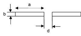
- Vacuum processing system according to any of the proceeding claims, whereby the heating means (5) comprises a plurality of rectangular heating elements (14) each having a length (c), a width (a) and a thickness (b), the heating elements (14) are electrically connected in series and/or in parallel, the heating elements (14) are arranged along their widths (a) and lengths (c) in a plane parallel to the substrate plane (4) forming the first plane surface (10) respectively the second plane surface (11) of the heating means (5), each heating element (14) comprises a width (a) that is ≥ 500 times of the thickness (b) of the respective heating element (14) and a length (c) that is ≥ 3000 times the thickness (b) of the respective heating element (14) and/or the heating elements (14) are arranged adjacent to each other with a distance (d) of 2 times ≥ the thickness of the respective heating element (14), preferably with a distance (d) of ≥ 4mm to each other.
- Vacuum processing system according to the proceeding claim, whereby the thickness (b) of the rectangular heating element (14) is ≤ 0,5mm, preferably ≤ 0,15mm.
- Vacuum processing system according to any of the proceeding claims, whereby the reflecting means (6, 7) comprises a material selected from the group consisting of copper, copper coating, nickel, nickel coating, gold, gold coating, silver, silver coating, aluminum and/or aluminum coating and/or the reflecting means (6, 7) comprises a reflecting surface having a surface roughness grade of ≤ N9.
- Vacuum processing system according to any of the proceeding claims, whereby the enclosure (1) is provided as a load lock comprising a sealable opening such that the enclosure (1) is accessible without breaking the vacuum when provided within the vacuum processing system.
- Method for operating a vacuum processing system according to any of the proceeding claims, comprising the steps of:a) Providing a plane substrate (2) having a surface size of ≥ 1 m2 into the enclosure (1) such that the substrate (2) is provided in the substrate plane (4),b) Evacuating the enclosure (1) to ≤ 8 * 10-2 mbar and to ≥ 1 * 10-5 mbar, andc) Providing electrical power of ≥ 26kW to the heating means (5) for heating the substrate (2).
- Method according to the proceeding claim, whereby during step c) the electrical power is provided such that the heating rate of the substrate (2) is ≥ 2,5K/s
- Method according to any of the two proceeding claims, whereby during step c) the substrate (2) is periodically or linearly moved within the enclosure (1).
Priority Applications (6)
| Application Number | Priority Date | Filing Date | Title |
|---|---|---|---|
| JP2013521130A JP6088970B2 (en) | 2010-07-27 | 2011-07-27 | Heating arrangement and method for heating a substrate |
| KR1020137004891A KR101783819B1 (en) | 2010-07-27 | 2011-07-27 | Heating arrangement and method for heating substrates |
| EP11761291.1A EP2599115B1 (en) | 2010-07-27 | 2011-07-27 | Heating arrangement and method for heating substrates |
| KR1020177027060A KR102121794B1 (en) | 2010-07-27 | 2011-07-27 | Heating arrangement and method for heating substrates |
| US13/812,289 US10276412B2 (en) | 2010-07-27 | 2011-07-27 | Heating arrangement and method for heating substrates |
| CN201180036622.4A CN103222041B (en) | 2010-07-27 | 2011-07-27 | For heater and the method for heated substrates |
Applications Claiming Priority (2)
| Application Number | Priority Date | Filing Date | Title |
|---|---|---|---|
| US36791010P | 2010-07-27 | 2010-07-27 | |
| US61/367,910 | 2010-07-27 |
Publications (1)
| Publication Number | Publication Date |
|---|---|
| WO2012013707A1 true WO2012013707A1 (en) | 2012-02-02 |
Family
ID=44681074
Family Applications (1)
| Application Number | Title | Priority Date | Filing Date |
|---|---|---|---|
| PCT/EP2011/062912 WO2012013707A1 (en) | 2010-07-27 | 2011-07-27 | Heating arrangement and method for heating substrates |
Country Status (6)
| Country | Link |
|---|---|
| US (1) | US10276412B2 (en) |
| EP (1) | EP2599115B1 (en) |
| JP (1) | JP6088970B2 (en) |
| KR (2) | KR101783819B1 (en) |
| CN (1) | CN103222041B (en) |
| WO (1) | WO2012013707A1 (en) |
Cited By (3)
| Publication number | Priority date | Publication date | Assignee | Title |
|---|---|---|---|---|
| WO2014032192A1 (en) * | 2012-08-27 | 2014-03-06 | Oc Oerlikon Balzers Ag | Processing arrangement with temperature conditioning arrangement and method of processing a substrate |
| US10208381B2 (en) | 2014-12-23 | 2019-02-19 | Rec Silicon Inc | Apparatus and method for managing a temperature profile using reflective energy in a thermal decomposition reactor |
| WO2022002382A1 (en) * | 2020-07-01 | 2022-01-06 | Applied Materials, Inc. | Method for operating a chamber, apparatus for processing a substrate, and substrate processing system |
Families Citing this family (5)
| Publication number | Priority date | Publication date | Assignee | Title |
|---|---|---|---|---|
| US20130074358A1 (en) * | 2011-09-24 | 2013-03-28 | Quantum Technology Holdings Limited | Heated body with high heat transfer rate material and its use |
| CN107109641B (en) * | 2014-12-23 | 2019-06-18 | 瑞科硅公司 | The device and method of Temperature Distribution can be managed using reflection in thermal decomposition reactor |
| KR102592972B1 (en) * | 2016-02-12 | 2023-10-24 | 삼성전자주식회사 | Sensing Module substrate and Sensing Module including the same |
| DE102016015502A1 (en) * | 2016-12-23 | 2018-06-28 | Singulus Technologies Ag | Process and device for the thermal treatment of coated substrates, in particular of thin-film solar substrates |
| DE102020130339A1 (en) * | 2020-11-17 | 2022-05-19 | Aixtron Se | Heating device for a CVD reactor |
Citations (3)
| Publication number | Priority date | Publication date | Assignee | Title |
|---|---|---|---|---|
| WO2000046840A1 (en) * | 1999-02-04 | 2000-08-10 | Steag Rtp Systems Gmbh | Cooled showerhead for rapid thermal processing (rtp) system |
| US6342691B1 (en) * | 1999-11-12 | 2002-01-29 | Mattson Technology, Inc. | Apparatus and method for thermal processing of semiconductor substrates |
| JP2010135531A (en) * | 2008-12-04 | 2010-06-17 | Shimadzu Corp | Vacuum heating device |
Family Cites Families (27)
| Publication number | Priority date | Publication date | Assignee | Title |
|---|---|---|---|---|
| US4470369A (en) * | 1982-07-12 | 1984-09-11 | Energy Conversion Devices, Inc. | Apparatus for uniformly heating a substrate |
| JPS63274714A (en) * | 1987-04-28 | 1988-11-11 | Michio Sugiyama | Radiant tube heater for vacuum heat treatment furnace |
| US4832778A (en) * | 1987-07-16 | 1989-05-23 | Texas Instruments Inc. | Processing apparatus for wafers |
| US5108570A (en) | 1990-03-30 | 1992-04-28 | Applied Materials, Inc. | Multistep sputtering process for forming aluminum layer over stepped semiconductor wafer |
| US5700992A (en) * | 1993-10-08 | 1997-12-23 | Toshiba Machine Co., Ltd. | Zigzag heating device with downward directed connecting portions |
| JPH07221037A (en) * | 1994-02-03 | 1995-08-18 | Dainippon Screen Mfg Co Ltd | Heat treating device |
| JPH0820868A (en) * | 1994-07-06 | 1996-01-23 | Noboru Naruo | Vacuum soaking heater |
| JPH08191074A (en) * | 1995-01-10 | 1996-07-23 | Touyoko Kagaku Kk | High speed thermal treatment equipment |
| JPH08222360A (en) * | 1995-02-10 | 1996-08-30 | Noboru Naruo | Equalized heater both for vacuum heating and for cooling |
| JPH10208855A (en) * | 1997-01-23 | 1998-08-07 | Toshiba Ceramics Co Ltd | Surface heater |
| JPH1197448A (en) * | 1997-09-18 | 1999-04-09 | Kemitoronikusu:Kk | Apparatus and method for heat treatment of semiconductor crystal |
| JP3170573B2 (en) * | 1999-06-23 | 2001-05-28 | 助川電気工業株式会社 | Disc heater for vertical heating furnace |
| JP2001332560A (en) * | 2000-05-23 | 2001-11-30 | Ibiden Co Ltd | Semiconductor manufacturing and inspecting device |
| JP2004146570A (en) * | 2002-10-24 | 2004-05-20 | Sumitomo Electric Ind Ltd | Ceramic heater for semiconductor manufacturing device |
| JP4227578B2 (en) * | 2003-09-30 | 2009-02-18 | キヤノン株式会社 | Heating method and image display device manufacturing method |
| JP4710255B2 (en) * | 2004-03-26 | 2011-06-29 | ウシオ電機株式会社 | Heating stage |
| JP4377296B2 (en) * | 2004-07-30 | 2009-12-02 | エア・ウォーター株式会社 | Deposition equipment |
| US20060127067A1 (en) * | 2004-12-13 | 2006-06-15 | General Electric Company | Fast heating and cooling wafer handling assembly and method of manufacturing thereof |
| TWI295816B (en) * | 2005-07-19 | 2008-04-11 | Applied Materials Inc | Hybrid pvd-cvd system |
| US7842135B2 (en) * | 2006-01-09 | 2010-11-30 | Aixtron Ag | Equipment innovations for nano-technology aquipment, especially for plasma growth chambers of carbon nanotube and nanowire |
| JP5041736B2 (en) * | 2006-06-09 | 2012-10-03 | キヤノントッキ株式会社 | Substrate heating apparatus and substrate heating method |
| JP4142706B2 (en) | 2006-09-28 | 2008-09-03 | 富士フイルム株式会社 | Film forming apparatus, film forming method, insulating film, dielectric film, piezoelectric film, ferroelectric film, piezoelectric element, and liquid discharge apparatus |
| US8057601B2 (en) * | 2007-05-09 | 2011-11-15 | Applied Materials, Inc. | Apparatus and method for supporting, positioning and rotating a substrate in a processing chamber |
| US8548311B2 (en) * | 2008-04-09 | 2013-10-01 | Applied Materials, Inc. | Apparatus and method for improved control of heating and cooling of substrates |
| US8961691B2 (en) * | 2008-09-04 | 2015-02-24 | Tokyo Electron Limited | Film deposition apparatus, film deposition method, computer readable storage medium for storing a program causing the apparatus to perform the method |
| US8294068B2 (en) * | 2008-09-10 | 2012-10-23 | Applied Materials, Inc. | Rapid thermal processing lamphead with improved cooling |
| US20100151680A1 (en) * | 2008-12-17 | 2010-06-17 | Optisolar Inc. | Substrate carrier with enhanced temperature uniformity |
-
2011
- 2011-07-27 US US13/812,289 patent/US10276412B2/en active Active
- 2011-07-27 JP JP2013521130A patent/JP6088970B2/en active Active
- 2011-07-27 KR KR1020137004891A patent/KR101783819B1/en active IP Right Grant
- 2011-07-27 CN CN201180036622.4A patent/CN103222041B/en active Active
- 2011-07-27 EP EP11761291.1A patent/EP2599115B1/en active Active
- 2011-07-27 WO PCT/EP2011/062912 patent/WO2012013707A1/en active Application Filing
- 2011-07-27 KR KR1020177027060A patent/KR102121794B1/en active IP Right Grant
Patent Citations (3)
| Publication number | Priority date | Publication date | Assignee | Title |
|---|---|---|---|---|
| WO2000046840A1 (en) * | 1999-02-04 | 2000-08-10 | Steag Rtp Systems Gmbh | Cooled showerhead for rapid thermal processing (rtp) system |
| US6342691B1 (en) * | 1999-11-12 | 2002-01-29 | Mattson Technology, Inc. | Apparatus and method for thermal processing of semiconductor substrates |
| JP2010135531A (en) * | 2008-12-04 | 2010-06-17 | Shimadzu Corp | Vacuum heating device |
Cited By (4)
| Publication number | Priority date | Publication date | Assignee | Title |
|---|---|---|---|---|
| WO2014032192A1 (en) * | 2012-08-27 | 2014-03-06 | Oc Oerlikon Balzers Ag | Processing arrangement with temperature conditioning arrangement and method of processing a substrate |
| CN104995727A (en) * | 2012-08-27 | 2015-10-21 | 欧瑞康先进科技股份公司 | Processing arrangement with temperature conditioning arrangement and method of processing a substrate |
| US10208381B2 (en) | 2014-12-23 | 2019-02-19 | Rec Silicon Inc | Apparatus and method for managing a temperature profile using reflective energy in a thermal decomposition reactor |
| WO2022002382A1 (en) * | 2020-07-01 | 2022-01-06 | Applied Materials, Inc. | Method for operating a chamber, apparatus for processing a substrate, and substrate processing system |
Also Published As
| Publication number | Publication date |
|---|---|
| KR101783819B1 (en) | 2017-10-10 |
| KR20170117198A (en) | 2017-10-20 |
| EP2599115A1 (en) | 2013-06-05 |
| US20140202027A1 (en) | 2014-07-24 |
| EP2599115B1 (en) | 2015-02-25 |
| CN103222041A (en) | 2013-07-24 |
| US10276412B2 (en) | 2019-04-30 |
| JP2013541176A (en) | 2013-11-07 |
| JP6088970B2 (en) | 2017-03-01 |
| KR20130105606A (en) | 2013-09-25 |
| CN103222041B (en) | 2016-01-20 |
| KR102121794B1 (en) | 2020-06-12 |
Similar Documents
| Publication | Publication Date | Title |
|---|---|---|
| EP2599115B1 (en) | Heating arrangement and method for heating substrates | |
| TWI449121B (en) | Substrate support regulating temperature of substrate and uses thereof | |
| US20110033638A1 (en) | Method and apparatus for deposition on large area substrates having reduced gas usage | |
| US8302554B2 (en) | Apparatus and method for rapid cooling of large area substrates in vacuum | |
| US20190390344A1 (en) | Process module | |
| WO2011075563A2 (en) | Substrate processing apparatus having a radiant cavity | |
| JP2013541176A5 (en) | ||
| US20080302653A1 (en) | Method And Device For Producing An Anti-Reflection Or Passivation Layer For Solar Cells | |
| WO2012028704A1 (en) | Substrate heating device | |
| EP1976022A2 (en) | Method and device for producing an anti-reflection or passivation layer for solar cells | |
| KR101720884B1 (en) | Avoidance of glass bending in thermal processes | |
| CN101822122A (en) | Apparatus for irradiation unit | |
| EP2896065A1 (en) | Processing arrangement with temperature conditioning arrangement and method of processing a substrate | |
| US20190295868A1 (en) | Heating assembly | |
| JP2008263189A (en) | Method of manufacturing anti-reflection or passivation layer for solar cell, and coating device | |
| JP4981477B2 (en) | Vacuum processing apparatus and substrate heating method | |
| JP5404322B2 (en) | Manufacturing method of multi-junction solar cell | |
| CN113574683A (en) | Device, apparatus and method for the thermal treatment of a multilayer body of a thin-film solar module | |
| CN219861549U (en) | Plate heater and heating cavity | |
| US20230245868A1 (en) | Holding device, and use of the holding device |
Legal Events
| Date | Code | Title | Description |
|---|---|---|---|
| 121 | Ep: the epo has been informed by wipo that ep was designated in this application |
Ref document number: 11761291 Country of ref document: EP Kind code of ref document: A1 |
|
| WWE | Wipo information: entry into national phase |
Ref document number: 2011761291 Country of ref document: EP |
|
| ENP | Entry into the national phase |
Ref document number: 2013521130 Country of ref document: JP Kind code of ref document: A |
|
| NENP | Non-entry into the national phase |
Ref country code: DE |
|
| ENP | Entry into the national phase |
Ref document number: 20137004891 Country of ref document: KR Kind code of ref document: A |
|
| WWE | Wipo information: entry into national phase |
Ref document number: 13812289 Country of ref document: US |