WO2012133716A1 - 有機el発光装置、有機el発光装置の製造方法及び有機el照明装置 - Google Patents
有機el発光装置、有機el発光装置の製造方法及び有機el照明装置 Download PDFInfo
- Publication number
- WO2012133716A1 WO2012133716A1 PCT/JP2012/058490 JP2012058490W WO2012133716A1 WO 2012133716 A1 WO2012133716 A1 WO 2012133716A1 JP 2012058490 W JP2012058490 W JP 2012058490W WO 2012133716 A1 WO2012133716 A1 WO 2012133716A1
- Authority
- WO
- WIPO (PCT)
- Prior art keywords
- organic
- light emitting
- contact portion
- electrode contact
- negative electrode
- Prior art date
Links
Images


Classifications
-
- H—ELECTRICITY
- H10—SEMICONDUCTOR DEVICES; ELECTRIC SOLID-STATE DEVICES NOT OTHERWISE PROVIDED FOR
- H10K—ORGANIC ELECTRIC SOLID-STATE DEVICES
- H10K50/00—Organic light-emitting devices
- H10K50/80—Constructional details
- H10K50/805—Electrodes
-
- H—ELECTRICITY
- H10—SEMICONDUCTOR DEVICES; ELECTRIC SOLID-STATE DEVICES NOT OTHERWISE PROVIDED FOR
- H10K—ORGANIC ELECTRIC SOLID-STATE DEVICES
- H10K50/00—Organic light-emitting devices
- H10K50/80—Constructional details
- H10K50/805—Electrodes
- H10K50/81—Anodes
- H10K50/814—Anodes combined with auxiliary electrodes, e.g. ITO layer combined with metal lines
-
- H—ELECTRICITY
- H10—SEMICONDUCTOR DEVICES; ELECTRIC SOLID-STATE DEVICES NOT OTHERWISE PROVIDED FOR
- H10K—ORGANIC ELECTRIC SOLID-STATE DEVICES
- H10K50/00—Organic light-emitting devices
- H10K50/80—Constructional details
- H10K50/84—Passivation; Containers; Encapsulations
-
- H—ELECTRICITY
- H10—SEMICONDUCTOR DEVICES; ELECTRIC SOLID-STATE DEVICES NOT OTHERWISE PROVIDED FOR
- H10K—ORGANIC ELECTRIC SOLID-STATE DEVICES
- H10K50/00—Organic light-emitting devices
- H10K50/80—Constructional details
- H10K50/84—Passivation; Containers; Encapsulations
- H10K50/844—Encapsulations
-
- H—ELECTRICITY
- H10—SEMICONDUCTOR DEVICES; ELECTRIC SOLID-STATE DEVICES NOT OTHERWISE PROVIDED FOR
- H10K—ORGANIC ELECTRIC SOLID-STATE DEVICES
- H10K71/00—Manufacture or treatment specially adapted for the organic devices covered by this subclass
-
- H—ELECTRICITY
- H10—SEMICONDUCTOR DEVICES; ELECTRIC SOLID-STATE DEVICES NOT OTHERWISE PROVIDED FOR
- H10K—ORGANIC ELECTRIC SOLID-STATE DEVICES
- H10K2102/00—Constructional details relating to the organic devices covered by this subclass
- H10K2102/301—Details of OLEDs
- H10K2102/341—Short-circuit prevention
Definitions
- the present invention relates to an organic EL light emitting device, a method for manufacturing the organic EL light emitting device, and an organic EL lighting device.
- An illuminating device including a light-emitting device using organic electroluminescence (hereinafter referred to as organic EL) has been used more frequently, such as being put to practical use in a mobile phone display.
- a lighting device using an organic EL has advantages such as energy saving, low heat generation, thin and light, and environmental friendliness as compared with a conventional lighting device such as a fluorescent lamp.
- the illumination range can be widened because of the surface light source, or when a plastic substrate is used, it can be applied to a lighting device with high designability. For this reason, it is expected not only in homes, offices, and car lighting devices, but also in decorative lighting and POP lighting.
- Patent Document 3 describes a planar light-emitting device that can reduce luminance unevenness and reduce the area of a non-light-emitting portion.
- the technology is that two predetermined parallel sides of the four sides of the rectangular light-emitting portion constituted by a region in which only the organic layer is interposed between the planar anode and the planar cathode and the outer peripheral edge of the transparent substrate Is smaller than the distance between the other two parallel sides and the outer peripheral edge of the transparent substrate, and the cathode feeding portion and the anode feeding portion are arranged along the other two parallel sides of the light emitting portion, and the cathode
- This is a technique in which anode power feeding units are arranged on both sides in the width direction of the power feeding unit.
- Patent Document 1 describes an organic EL element having a light emitting region with a narrow width of an electrode wiring pattern in which an extraction terminal for an anode and a cathode is installed on the short side of a transparent substrate. Further, in Patent Document 2, the cathode has a lower electrical resistance than the anode, and the luminance unevenness can be reduced by making the surface of the anode terminal connected to the outside larger than the surface of the cathode terminal connected to the outside. An organic EL element is described.
- a related process of manufacturing an organic EL light emitting device is generally performed on a substrate with a transparent conductive electrode film such as ITO (Indium Tin Oxide), an electrode, an interlayer insulating film, and a photosensitive organic material. Insulators are formed sequentially.
- ITO Indium Tin Oxide
- the etching process during the process roughens the ITO surface and the ITO edge, causing a short circuit during use and causing defects.
- the process is complicated and very expensive.
- the organic EL light emitting device voltage is applied from the positive electrode and the negative electrode, carriers are injected, and light is emitted.
- the electrode portion generally uses each side, but an electrode extraction portion must be formed on each side. That part was a non-light emitting part.
- a so-called panel with a large frame portion and a low aperture ratio causes a decrease in total luminous flux and a decrease in illuminance, which is disadvantageous compared to other light sources. .
- the organic EL light emitting device is used as a backlight for, for example, a bulletin board or an advertisement display other than lighting, or when used for a curved lighting device.
- the present invention has been made in view of the above circumstances, and provides an organic EL light-emitting device, an organic EL light-emitting device manufacturing method, and an organic EL lighting device that are easy in process and capable of increasing the aperture ratio.
- the purpose is to do.
- the organic EL light emitting device is: A transparent substrate, A transparent electrode film formed on the substrate; A portion of the transparent electrode film, a positive electrode contact portion electrically connected to the transparent electrode film; An insulator layer formed by opening a light emitting portion on the transparent electrode film; An organic light emitting layer formed on the transparent electrode film and the insulator layer; A negative electrode layer formed on the organic light emitting layer; A negative electrode contact portion in contact with at least a part of the negative electrode layer and electrically connected to the negative electrode layer; A protective layer formed between the transparent electrode film and the positive electrode contact part, and the negative electrode contact part to separate and electrically insulate; With The positive electrode contact part and the negative electrode contact part are electrically insulated by the insulator layer or the protective layer, The transparent electrode film covers the entire range of the positive electrode contact portion, the insulator layer, the organic light emitting layer, the negative electrode layer, the negative electrode contact portion, and the protective layer on the substrate. It is characterized by being formed without gaps.
- the manufacturing method of the organic EL light emitting device includes: Forming a transparent electrode film on a transparent substrate; Forming a positive electrode contact portion electrically connected to the transparent electrode film in a part of the transparent electrode film; Forming a negative electrode contact portion in a part above the transparent electrode film, spaced apart from the transparent electrode film and the positive electrode contact portion; Forming an insulator layer by opening a light emitting part on the transparent electrode film; Forming an organic light emitting layer on the transparent electrode film and the insulator layer; Forming on the organic light emitting layer a negative electrode layer that is electrically connected to the negative electrode contact portion and spaced apart from the transparent electrode film and the positive electrode contact portion; With Before the step of forming the negative electrode contact portion, Forming a protective layer between the transparent electrode film, the positive electrode contact portion, and the negative electrode contact portion to electrically insulate the transparent electrode film, the positive electrode contact portion, and the negative electrode contact portion; It is characterized by providing.
- the organic EL lighting device is: An organic EL light emitting device according to the first aspect of the present invention is provided.
- the organic EL lighting device is: The organic EL light-emitting device manufactured with the manufacturing method of the organic EL light-emitting device which concerns on the 2nd viewpoint of this invention is provided.
- the process is easy and the aperture ratio can be increased.
- FIG. 2 is a configuration cross-sectional view of the organic EL light emitting device according to Embodiment 1, showing a cross section taken along line X1-X1 in FIG. 1F.
- FIG. 2 is a configuration cross-sectional view of the organic EL light emitting device according to Embodiment 1, showing a cross section taken along line Y1-Y1 of FIG. 1F. It is a structure sectional view showing a modification of the organic EL light emitting device shown in FIG. 3A.
- FIG. 4 is a structural cross-sectional view of an organic EL light emitting device according to Embodiment 2, showing a cross section taken along line Y2-Y2 of FIG. 4F.
- FIG. 4 is a structural cross-sectional view of an organic EL light emitting device according to Embodiment 2, showing a cross section taken along line Y2-Y2 of FIG. 4F.
- FIG. 5 is a structural cross-sectional view of an organic EL light emitting device according to Embodiment 2, showing a cross-sectional portion taken along line X2-X2 in FIG. 4F.
- FIG. 5 is a configuration plan view showing a different configuration of an organic EL light emitting device according to Embodiment 2.
- FIG. FIG. 7 is a configuration cross-sectional view of a different configuration of the organic EL light emitting device according to Embodiment 2, showing a cross section taken along line Y3-Y3 of FIG.
- FIG. 7 is a configuration cross-sectional view of a different configuration of the organic EL light emitting device according to Embodiment 2, showing a cross section taken along line Y3-Y3 of FIG.
- It is a structure top view which shows an example of the manufacturing process of the organic electroluminescent light emitting device concerning Embodiment 3 of this invention.
- FIG. 1 It is a structure top view which shows an example of the manufacturing process of the organic electroluminescent light emitting device concerning Embodiment 3 of this invention. It is a structure top view which shows an example of the manufacturing process of the organic electroluminescent light emitting device concerning Embodiment 3 of this invention. It is a structure top view which shows an example of the manufacturing process of the organic electroluminescent light emitting device concerning Embodiment 3 of this invention. It is a structure top view which shows an example of the manufacturing process of the organic electroluminescent light emitting device concerning Embodiment 3 of this invention. It is a structure top view which shows an example of the manufacturing process of the organic electroluminescent light emitting device concerning Embodiment 3 of this invention. FIG.
- FIG. 8 is a structural cross-sectional view of an organic EL light emitting device according to Embodiment 3, showing a cross section taken along line X4-X4 of FIG. 8F.
- FIG. 8 is a structural cross-sectional view of an organic EL light emitting device according to Embodiment 3, showing a cross section taken along line X4-X4 of FIG. 8F.
- FIG. 8 is a structural cross-sectional view of an organic EL light emitting device according to Embodiment 3, showing a cross section taken along line Y4-Y4 of FIG. 8F. It is a structure top view which shows an example of the manufacturing process of the organic electroluminescent light-emitting device which concerns on the modification of Embodiment 3 of this invention.
- FIG. 10 is a structural cross-sectional view of an organic EL light emitting device according to a modification of Embodiment 3, showing a cross section taken along line Y5-Y5 in FIG. 11F. It is a structure top view which shows an example of the manufacturing process of the organic electroluminescent light emitting device concerning Embodiment 4 of this invention. It is a structure top view which shows an example of the manufacturing process of the organic electroluminescent light emitting device concerning Embodiment 4 of this invention.
- FIG. 1A to 1F are configuration plan views showing an example of manufacturing steps of the organic EL light emitting device according to Embodiment 1 of the present invention.
- FIG. 2 is a structural cross-sectional view of the organic EL light emitting device according to Embodiment 1, and shows a cross section taken along line X1-X1 of FIG. 1F.
- FIG. 3A is a structural cross-sectional view of the organic EL light emitting device according to Embodiment 1, and shows a cross section taken along line Y1-Y1 of FIG. 1F.
- FIG. 3B shows a modification of FIG. 3A.
- the light emission principle of organic EL is that when a voltage is applied to the cathode and the anode, electrons and holes injected from each recombine in the light emitting layer, thereby forming excitons and becoming excited. This mechanism emits light when returning to a low energy level (such as a ground state).
- a low energy level such as a ground state
- an excited state having the same electron spin multiplicity as the ground state is a singlet excited state
- an excited state having a different electron spin multiplicity is a triplet excited state.
- Luminescence is obtained when returning from this excited state to a low level or ground state, and fluorescence is obtained from the singlet excited state, and phosphorescence is obtained from the triplet excited state.
- the light-emitting layer is a two-component system including a host and a dopant, the excited state generated by the host molecule transfers energy to the dopant molecule, and the dopant molecule emits light.
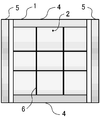
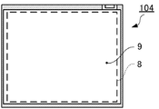
- the organic EL light emitting device 100 includes a substrate 1, a transparent electrode film (positive electrode film) 2, a protective layer 3, a positive electrode contact / power supply unit 4 (hereinafter referred to as a positive electrode contact unit 4), and a negative electrode contact / power supply unit 5 (hereinafter referred to as a positive electrode contact / power supply unit 5).
- the organic EL light emitting device 100 is used for an organic EL lighting device (lighting device) such as a room lamp.
- the organic EL light emitting device 100 is not limited to a lighting device, and may be used in various applications such as a bulletin board, an information display panel for advertisements, an image display, a liquid crystal display backlight, a display device used for home appliances, and the like. Is available.
- the positive electrode contact / power supply unit 4 also serves as the positive electrode contact unit 4 and a power supply unit that supplies power to the organic light emitting layer 8 via the positive electrode contact unit 4.
- the negative electrode contact / power supply unit 5 also serves as the negative electrode contact unit 5 and a power supply unit that supplies power to the organic light emitting layer 8 via the negative electrode contact unit 5.
- the substrate 1 is formed of a material such as non-alkali glass, for example. Further, a flexible resin substrate such as PEN (polyethylene naphthalate) may be used.
- PEN polyethylene naphthalate
- the transparent electrode film 2 is made of, for example, indium tin oxide (ITO) or the like, and is formed on almost the entire surface of the substrate 1 without any gaps by sputtering or the like.
- the almost entire surface on the substrate 1 includes a range in which the protective layer 3, the positive electrode contact portion 4, the negative electrode contact portion 5, the auxiliary electrode 6, the insulator layer 7, the organic light emitting layer 8, and the negative electrode film 9 are formed. Refers to the entire range.
- the transparent electrode film 2 includes the protective layer 3, the positive electrode contact portion 4, the negative electrode contact portion 5, the auxiliary electrode 6, the insulator layer 7, the organic light emitting layer 8, and the negative electrode in plan view on the substrate 1. It is formed over the entire region including at least the region (range) where the film 9 is formed.
- the transparent electrode film 2 may be formed so as to cover the entire surface without gaps to the edge of the substrate 1 or may not be completely covered up to the edge of the substrate 1, but at least the protective layer 3, the positive electrode contact portion 4, the negative electrode A transparent electrode film 2 is formed below the contact portion 5, the auxiliary electrode 6, the insulator layer 7, the organic light emitting layer 8, and the negative electrode film 9.
- the transparent electrode film 2 may be formed by another physical vapor deposition method (PVD: Physical Vapor Deposition) such as a vacuum vapor deposition method.
- PVD Physical Vapor Deposition
- the thickness of the transparent electrode film 2 can be set to 100 to 300 nm, for example.
- the protective layer 3 is formed on the transparent electrode film 2 and the like, and is used to form a base for lift-up while insulating the layers.
- the protective layer 3 also serves as a planarizing film below the protective layer 3.
- a photosensitive photoresist material such as novolac, acrylic, or polyimide material, or an inorganic material film such as a silicon nitride (SiNx) film or a silicon oxide (SiOx) film is used.
- the protective layer 3 can be formed by patterning by photolithography after coating, or by patterning by shadow mask or photoetching using a vacuum vapor deposition method or a chemical vapor deposition method (CVD: Chemical Vapor Deposition). .
- the transparent electrode film 2 is formed on the substrate 1, and the negative electrode contact portion 5 is formed on the protective layer 3.
- the formed height refers to the position of each layer of the positive electrode contact portion 4 and the negative electrode contact portion 5 from the substrate 1.
- the difference in height between the positive electrode contact portion 4 and the negative electrode contact portion 5 is hereinafter referred to as forming with different layers.
- the formation of the different layers also includes forming the positive electrode contact portion 4 and the negative electrode contact portion 5 by different process steps (order).
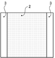
- the protective layer 3 is formed on opposite ends of the transparent electrode film 2 so as to border the organic EL light emitting device 100.
- the protective layer 3 is formed along the left and right opposing sides.
- a negative electrode contact portion 5 is formed at the end of the transparent electrode film 2 on the side where the protective layer 3 is to be formed.
- the negative electrode contact portion 5 is formed on the protective layer 3 so as to provide a gap on the center side of the transparent electrode film 2. As shown in FIGS.
- the negative electrode contact portion 5 is formed to be narrower than the protective layer 3, and is retracted by a predetermined distance from the center of the transparent electrode film 2 as compared with the protective layer 3. Yes.
- the negative electrode contact portion 5 narrower than the protective layer 3 on the protective layer 3, the positive electrode contact portion 4 and the negative electrode contact portion 5 can be easily separated even when not formed with high accuracy. it can.
- the film thickness can be set to, for example, 500 to 1500 nm.
- the positive electrode contact portion 4 is electrically connected to the transparent electrode film 2 and injects holes supplied to the organic EL light emitting device 100 into the transparent electrode film 2 through the positive electrode contact portion 4.
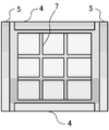
- the positive electrode contact portion 4 is formed to face the end portion on the transparent electrode film 2 on the side where the protective layer 3 is not formed. In this embodiment, as shown to FIG. 1C, it forms along the up-and-down opposing side.
- the positive electrode contact portion 4 is made of a metal material such as Cr (chromium), Mo—Nd (molybdenum-neodymium), or Mo—Al—Mo (molybdenum-aluminum-molybdenum).
- the positive electrode contact portion 4 may be formed by a method such as sputtering using a shadow mask or the like, or photoetching may be performed after the entire surface is formed.
- the negative electrode contact portion 5 is electrically connected to the negative electrode film 9 and injects electrons supplied to the organic EL light emitting device 100 into the negative electrode film 9 through the negative electrode contact portion 5.
- the negative electrode contact portion 5 is formed on the protective layer 3 formed in advance on the transparent electrode film 2.
- the protective layer 3 is a base for lift-up, and is used to form a different layer so that the negative electrode contact portion 5 is not electrically connected to the positive electrode contact portion 4.
- the protective layer 3 also serves as an interlayer insulator, the positive electrode contact portion 4 and the negative electrode contact portion 5 located above and below the protective layer 3 are not short-circuited. Further, since the positive electrode contact portion 4 and the negative electrode contact portion 5 are formed in different layers, the arrangement of the transparent electrode film 2 connected to the positive electrode contact portion 4 and the negative electrode film 9 connected to the negative electrode contact portion 5 is An arrangement in which electrical contact is unlikely to occur easily can be achieved.
- the same metal material as that of the positive electrode contact portion 4 can be used for the negative electrode contact portion 5.
- the negative electrode contact portion 5 may be formed by a method such as sputtering using a shadow mask or the like, or photoetching may be performed after the entire surface is formed.
- the positive electrode contact portion 4 and the negative electrode contact portion 5 can be simultaneously formed at the same time in the same process, so that the number of steps is not increased and the process load can be reduced.
- the auxiliary electrode 6 is electrically connected to the positive electrode contact portion 4 through the transparent electrode film 2 or directly.
- the auxiliary electrode 6 is made of a metal material such as Cr (chromium), Mo—Nd (molybdenum-neodymium), or Mo—Al—Mo (molybdenum-aluminum-molybdenum).
- the auxiliary electrode 6 is formed on the transparent electrode film 2 by a method such as sputtering using a shadow mask or the like.
- the auxiliary electrode 6 may be formed by performing photo-etching into an arbitrary shape after film formation with a metal material.
- the auxiliary electrode 6 is electrically connected to the positive electrode contact portion 4 via the transparent electrode film 2 or directly.
- the shape of the auxiliary electrode 6 is not limited to this.
- the positive electrode contact portion 4 and the auxiliary electrode 6 can be formed simultaneously in the same process, and the number of steps is not increased, and the process load can be reduced.
- the positive electrode contact portion 4 and the auxiliary electrode 6 may be simultaneously formed by a method such as sputtering or photo-etching into an arbitrary shape after film formation with a metal material.
- the positive electrode contact portion 4 and the auxiliary electrode 6 may be formed simultaneously.
- the positive electrode contact portion 4 and the negative electrode contact portion 5 can be easily formed at the same time because the protective layer 3 and / or an insulator layer 7 described later serve as a mask and can be reliably separated at the time of formation. By forming them simultaneously, the number of steps can be reduced.
- the film thicknesses of the positive electrode contact portion 4, the negative electrode contact portion 5, and the auxiliary electrode 6 can be set to 200 to 1000 nm, for example.
- the organic EL light emitting device 100 emits light on the light emitting surface by injecting electrons and holes into the light emitting element and recombining them.
- the auxiliary electrode 6 reduces the voltage drop due to the wiring resistance of the transparent electrode film 2 having a high sheet resistance, facilitates uniform hole supply to the light emitting surface of the organic EL light emitting device 100, and causes in-plane luminance variations. Suppress and maintain stable light emission.
- the insulator layer 7 is formed along the positive electrode contact portion 4 and the negative electrode contact portion 5, and is further formed between the positive electrode contact portion 4 and the negative electrode contact portion 5 and on the auxiliary electrode 6.
- the insulator layer 7 is formed by opening the light emitting portion in order to make the light emitting portion of the organic EL light emitting device 100 into a predetermined shape. For example, as shown in FIG. 1D, a portion formed along each of the positive electrode contact portion 4 and the negative electrode contact portion 5 forms an opening, and a region inside the opening is a light emitting portion of the organic EL light emitting device 100. is there. A part of the insulator layer 7 is formed in a lattice shape so as to further cover the auxiliary electrode 6 inside the opening.
- the insulator layer 7 also serves as a lower planarizing film.
- the same material as that of the protective layer 3 can be selected.
- Photosensitive photoresist materials such as novolac, acrylic, and polyimide materials, silicon nitride (SiNx) films, silicon oxide (SiOx) films, and the like can be used.
- An inorganic material film is used.
- the insulator layer 7 may be formed by patterning by photolithography after coating, or by patterning by shadow mask or photoetching using a vacuum vapor deposition method or a chemical vapor deposition method (CVD: Chemical Vapor Deposition). it can.
- the film thickness when a resist material is used for the insulator layer 7 can be set to 500 to 1500 nm, for example, and the film thickness when an inorganic material is used can be set to 200 to 600 nm, for example.
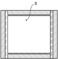
- the organic light emitting layer 8 has a role of a light emitting layer, and is formed on the transparent electrode film 2 and the insulator layer 7 where the insulator layer 7 is not formed. At this time, as long as the organic light emitting layer 8 is formed in a portion surrounded by the insulator layer 7, a part of the organic light emitting layer 8 may be formed on the insulator layer 7. Since the insulator layer 7 serves as a mask, it can be patterned in a self-aligning manner. There is no need to directly connect the transparent electrode film 2 and the negative electrode contact portion 5 via the organic light emitting layer 8. At this time, the organic light emitting layer 8 preferably includes a hole injection / transport layer such as a triphenylamine derivative on the transparent electrode film 2. The organic light emitting layer 8 may further include an electron transport layer such as a triazole derivative between the negative electrode film 9.
- the negative electrode film 9 is formed on the organic light emitting layer 8.
- the negative electrode film 9 is electrically connected to the negative electrode contact portion 5 and injects electrons supplied to the organic EL light emitting device 100 into the negative electrode film 9 through the negative electrode contact portion 5.
- the negative electrode film 9 is formed of a metal material such as Al (aluminum).
- an electron injection layer such as LiF (lithium fluoride) may be provided, and the negative electrode film 9 may be formed thereon.
- the film thickness of the negative electrode film 9 can be set to, for example, 50 to 300 nm.
- power supply from the power source to the negative electrode layer 9 may be provided anywhere.
- the negative electrode film 9 may be formed so that the outer peripheral portion is thick, and power may be supplied from four directions.
- the organic light emitting layer 8 includes a hole injection layer, a hole transport layer, and an electron transport layer in addition to the light emitting layer, the transparent electrode film 2 to the hole injection layer, the hole transport layer, the light emitting layer, and the electron transport layer are used. It is desirable that the layers are sequentially formed in this order. In order to improve the recombination probability and consequently the emission quantum efficiency, a hole blocking layer may be used between the light emitting layer and the electron transport layer. Further, the organic light emitting layer 8 is not limited to a single light emitting layer, and the light emitting layer may have two layers. The configuration of the organic light-emitting layer 8 can be changed as appropriate.
- the organic light-emitting layer 8 may be formed from the transparent electrode film 2 in the order of the light-emitting layer and the electron transport layer. .
- the transparent electrode film 2 may be formed in the order of the hole injection / transport layer and the light emitting layer.
- the organic light emitting layer 8 may be a single layer including only the light emitting layer. In the present embodiment, the total film thickness of the organic light emitting layer 8 can be set to 100 to 500 nm, for example.
- a transparent electrode film 2 made of a transparent conductive material such as indium tin oxide (ITO) is formed on a substrate 1 made of a material such as non-alkali glass. Form uniformly on the entire surface.
- the transparent electrode film 2 is formed by physical vapor deposition (PVD) such as sputtering or vacuum vapor deposition.
- the protective layer 3 is formed on the opposite side edges of the transparent electrode film 2 (see FIG. 1B).
- a base lifted up from the transparent electrode film 2 is formed by the protective layer 3 portion, and the negative electrode contact portion 5 and the positive electrode contact portion 4 formed in FIG. 1C can be formed in different layers. Can be easily separated.
- the negative electrode contact portion 5 is formed on the protective layer 3, and the positive electrode contact portion 4 is formed on the transparent electrode film 2 on the opposite side edge portion of the transparent electrode film 2 on which the protective layer 3 is not formed.
- the auxiliary electrode 6 is formed on the transparent electrode film 2.
- the positive electrode contact portion 4, the negative electrode contact portion 5 and the auxiliary electrode 6 are made of, for example, a metal material such as Cr (chromium), Mo—Nd (molybdenum-neodymium), Mo—Al—Mo (molybdenum-aluminum-molybdenum), It is formed by sputtering using a shadow mask or the like. Alternatively, photoetching may be performed after the metal material is formed.
- the organic EL light emitting device 100 is formed so as to be electrically connected to a power source connected to the outside of the organic EL light emitting device 100 through the positive electrode contact portion 4.
- the organic EL light emitting device 100 is organic through the negative electrode contact portion 5.
- the EL light emitting device 100 is formed so as to be electrically connected to a power source connected to the outside.
- the protective layer 3 is formed in advance, and the negative electrode contact portion 5 is formed thereon, whereby the positive electrode contact portion 4 and the negative electrode contact portion 5 are formed in different layers to facilitate electrical insulation.
- the insulator layer 7 is integrally formed simultaneously with, for example, a photoresist.
- the insulator layer 7 is formed on the auxiliary electrode 6. Further, the insulator layer 7 covers other than the light emitting surface in accordance with the light emission shape of the organic EL light emitting device 100. Furthermore, the insulator layer 7 is formed between the positive electrode contact portion 4 and the negative electrode contact portion 5 and between the transparent electrode film 2 and the negative electrode contact portion 5 to maintain electrical insulation and prevent a short circuit.
- the insulator layer 7 may be formed of a photoresist which is a photosensitive material, and is formed of an inorganic film material such as SiNx or SiOx by vacuum evaporation or CVD, and by a shadow mask or photoetching. It may be patterned and formed.
- an organic light emitting layer 8 is formed on the transparent electrode film 2 on which the insulator layer 7 is formed in FIG. 1D.
- the organic light emitting layer 8 is formed so that the transparent electrode film 2 and the negative electrode contact portion 5 are not electrically connected directly via the organic light emitting layer 8.
- the organic light emitting layer 8 is formed so as to partially overlap, for example, a part of the periphery, on the insulator layer 7 having a predetermined width formed so as to cover the outer periphery of the transparent electrode film 2. Can do. Since the insulator layer 7 serves as a mask, the need for a shadow mask with high alignment accuracy is eliminated, and the process can be facilitated. As shown in FIGS. 2 and 3, it is understood that the organic light emitting layer 8 may be formed on the insulating layer 7 having a width, and position adjustment with high accuracy is unnecessary.
- FIG. 3B is a configuration cross-sectional view of the organic EL light-emitting device, and shows a variation of the configuration cross-sectional view of the organic EL light-emitting device shown in FIG. 3A.
- the organic EL light emitting device 100 is formed so that the insulator layer 7 covers a part of the positive electrode contact portion 4, but as shown in FIG. 3B, the positive electrode contact portion 4 and the insulator layer 7 are formed. May be formed adjacent to each other. A gap may be formed between the positive electrode contact portion 4 and the insulator layer 7 as shown on the right side of FIG. 3B.
- the negative electrode film 9 can be formed on the organic light emitting layer 8, and the manufacturing process of the organic EL light emitting device 100 can be completed. As shown in FIG. 2, the negative electrode film 9 covers a part of the negative electrode contact portion 5 and is electrically connected to a power source connected to the outside of the organic EL light emitting device 100 via the negative electrode contact portion 5. Form to connect. Further, the negative electrode film 9 is formed so as not to be in direct contact with the positive electrode contact portion 4 and further not to be directly connected to the positive electrode contact portion 4. At this time, the negative electrode film 9 is formed so as to partially overlap, for example, a part of the periphery, on the insulator layer 7 having a predetermined width formed so as to cover the outer periphery of the transparent electrode film 2.
- the insulator layer 7 serves as a mask, the need for a shadow mask with high alignment accuracy is eliminated, and the process can be facilitated. As shown in FIG. 3, it can be seen that the negative electrode film 9 may be formed on the insulating layer 7 having a width, and position adjustment with high accuracy is unnecessary.
- the process is easy and the aperture ratio can be increased. Specifically, since the positive electrode and the negative electrode are reliably insulated from each other by the protective layer and the insulator layer, the process is easy and the positive electrode contact portion and the negative electrode contact portion can be narrowed to increase the aperture ratio. Is possible.
- the shape of the transparent electrode film such as ITO can be simplified, and a short circuit can be prevented while eliminating the need for high alignment accuracy, thereby reducing the total number of steps. It is also possible.
- the organic EL light-emitting device can have a predetermined light emission shape by covering the transparent electrode film with a protective film or the like without forming the transparent electrode film in a light emission shape. Therefore, it is not necessary to pattern the transparent electrode film by photoetching or the like, and the surface of the transparent electrode film is not uneven or rough. As a result, not only the process is simplified, but a short circuit does not occur, leading to a reduction in the defect rate.
- the positive electrode contact part and the negative electrode contact part in different layers, there is no possibility of short circuit due to contact. Also, the positive electrode transparent electrode film and the positive electrode contact part, and the negative electrode film and the negative electrode contact part can be reliably connected, and by connecting with each electrode part formed in an arbitrary shape, a large opening can be obtained. An organic EL light emitting device can be formed. Furthermore, the frame can be narrowed by designing the organic EL light emitting device, so that the total luminous flux can be improved and the power can be saved.
- FIG. 5 is a configuration cross-sectional view of the organic EL light emitting device according to the second embodiment.
- 5A and 5B show a cross section taken along line Y2-Y2 of FIG. 4F.
- FIG. 5C shows a cross-sectional portion taken along line X2-X2 of FIG. 4F.
- the positive electrode contact portion 4 is provided in the periphery, and power is supplied from four directions.
- the transparent electrode film 2 is formed without gaps in the entire range including the range of the layers other than the transparent electrode film 2 on the substrate, and the positive electrode contact portion 4 and the negative electrode contact portion 51 are different layers. Is formed in the same manner as the organic EL light emitting device 100 according to the first embodiment.
- the organic EL light emitting device 101 covers the positive electrode contact portion 4 that also serves as a power supply unit to the organic EL element with a protective layer (insulator layer 7), and the organic EL on the protective layer (insulator layer 7).
- a negative electrode contact portion 5 that also serves as a power supply portion to the element and a negative electrode contact / negative electrode extraction portion 51 (hereinafter, referred to as a negative electrode extraction portion 51) are stacked.
- the protective layer 3 and the insulator layer 7 of the first embodiment can be formed integrally with the same material at the same time (in the same process). 4C to 4F, the insulator layer 7 is described so as to include the protective layer 3.
- the insulator layer 7 has the function of the protective layer 3 in the first embodiment (the transparent electrode film and the positive electrode contact portion are separated from the negative electrode contact portion and electrically insulated). ing.
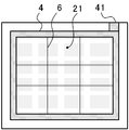
- the organic EL light emitting device 101 includes a substrate 1, a transparent electrode film (positive electrode film) 2, a positive electrode contact portion 4, a positive electrode contact hole / positive electrode extraction portion 41 (hereinafter referred to as a positive electrode contact hole portion 41), a negative electrode extraction portion. 51, an auxiliary electrode 6, an insulator layer 7, an organic light emitting layer 8, and a negative electrode film 9.
- the transparent electrode film 2 is uniformly formed on the entire surface of the substrate 1 as shown in FIG. 4A.
- a positive electrode contact portion 4 is formed in a ring shape around the transparent electrode film 2, and an auxiliary electrode 6 is formed on the transparent electrode film 2 (see FIG. 4B).
- the insulator layer 7 is formed so as to cover the positive electrode contact portion 4 and the auxiliary electrode 6.
- the insulator layer 7 is formed by opening the light emitting portion in accordance with the light emission shape of the organic EL light emitting device 101.
- a portion where the transparent electrode film 2 is exposed at the opening of the insulator layer 7 shown in FIG. 4C is a light emitting portion.
- the positive electrode contact hole portion 41 is not covered with the insulator layer 7 on the positive electrode contact portion 4 to form the positive electrode contact hole portion 41 (see FIG. 4C). Since this step can be performed simultaneously with the process of patterning the insulator layer 7, the number of process steps does not increase.
- the organic light emitting layer 8 is formed so as to cover the entire portion of the transparent electrode film 2 that is not covered with the positive electrode contact portion 4, the auxiliary electrode 6, and the insulator layer 7.
- a negative electrode film 9 is formed so as to cover the organic light emitting layer 8. Then, at least part of the negative electrode film 9 is in contact with the negative electrode extraction portion 51 to be electrically connected, and the manufacture of the organic EL light emitting device 101 is completed (see FIG. 4F).
- the negative electrode extraction portion 51 is formed so as to be in contact with the periphery of the negative electrode film 9 and to surround almost the entire periphery of the negative electrode film 9. In this way, since the negative electrode film 9 can be evenly fed from four sides, the luminance unevenness of the light emission of the organic light emitting layer 8 is reduced.
- the organic light emitting layer 8 and the negative electrode film 9 can be formed by overlapping a part, for example, a part in a circumferential shape, on the insulator layer 7 having a predetermined width. As a result, a shadow mask with high alignment accuracy is not necessary, and the process can be facilitated.
- FIGS. 5A and 5C show a case where the organic light emitting layer 8 is not interposed between the positive electrode contact portion 4 and the negative electrode film 9.
- FIG. 5B shows a cross section when the organic light emitting layer 8 protrudes from the opening of the insulator layer 7 to the position of the positive electrode contact portion 4.
- the negative electrode film 9 and the negative electrode extraction portion 51 are formed on the insulator layer 7. It can be formed to the edge.
- FIG. 6 is a configuration plan view showing a different configuration of the organic EL light emitting device according to the second embodiment.
- the negative electrode extraction portion 51 is provided at a corner adjacent to the positive electrode contact hole portion 41.
- the negative electrode extraction part 51 can be set at an arbitrary position as long as it is in contact with at least a part of the negative electrode film 9.
- FIGS. 7A and 7B are configuration cross-sectional views of different configurations of the organic EL light emitting device according to Embodiment 2, showing a cross section taken along line Y3-Y3 in FIG. 7A and 7B, since the positive electrode contact portion 4, the negative electrode film 9, and the negative electrode extraction portion 51 are formed of different layers, the negative electrode film 9 and the negative electrode extraction portion 51 are formed on the insulator layer 7. It can be formed to the edge. As can be seen from FIGS. 4 to 7, as long as the positive electrode contact hole portion 41 does not overlap the negative electrode film 9 or the negative electrode extraction portion 51, the positive electrode contact hole portion 41 and the negative electrode extraction portion 51 can be freely arranged.
- the process is easy and the aperture ratio can be increased.
- the shape of the transparent electrode film such as ITO can be simplified, and a short circuit can be prevented while eliminating the need for a high degree of alignment accuracy, thereby reducing the total number of steps. It is also possible. Further, the positive electrode contact portion can be formed so as to surround the four sides, and the in-plane luminance variation can be reduced.
- FIGS. 3) 8A-8F are configuration plan views showing an example of the manufacturing process of the organic EL light emitting device according to Embodiment 3 of the present invention.
- 9A and 9B are configuration cross-sectional views of the organic EL light emitting device according to Embodiment 3, and show a cross section taken along line X4-X4 in FIG. 8F.
- FIG. 10 is a structural cross-sectional view of the organic EL light emitting device according to Embodiment 3, and shows a cross section taken along line Y4-Y4 of FIG. 8F.
- the negative electrode contact portion 5 is formed on the positive electrode contact portion 4 with the protective layer 3 interposed therebetween.
- the transparent electrode film 2 is formed without gaps in the entire range including the range where layers other than the transparent electrode film 2 are formed on the substrate, and the positive electrode contact portion 4 and the negative electrode contact portion 5. Is formed in a different layer, similar to the organic EL light emitting device 100 according to the first embodiment.
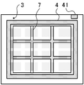
- the organic EL light emitting device 102 includes a substrate 1, a transparent electrode film (positive electrode film) 2, a positive electrode contact portion 4, a positive electrode contact hole portion 41, a negative electrode contact portion 5, an auxiliary electrode 6, an insulator layer 7, an organic light emitting layer 8, And a negative electrode film 9.
- the transparent electrode film 2 is uniformly formed on the entire surface of the substrate 1 on the substrate 1.
- the positive electrode contact portion 4 is formed in a ring shape so as to surround the periphery of the transparent electrode film 2, and the auxiliary electrode 6 is formed on the transparent electrode film 2.
- the positive electrode contact portion 4 and the auxiliary electrode 6 may be formed simultaneously (see FIG. 8B).
- the protective layer 3 is formed, for example, in an annular shape so as to cover the positive electrode contact portion 4 except for a part of the positive electrode contact portion 4.
- the inside surrounded by the protective layer 3 (the inside of the opening of the protective layer 3) becomes the light emission shape (light emitting part) of the organic EL light emitting device 102.
- the protective layer 3 is formed by opening the light emitting portion, and has the function of the insulator layer 7 of the first embodiment.
- the insulator layer 7 is formed in a lattice shape so as to cover the auxiliary electrode 6 (see FIG. 8C).
- the protective layer 3 is formed except for a part of the positive electrode contact portion 4, and an electrode extraction portion for supplying power from the positive electrode contact portion 4 is secured.
- the protective layer 3 and the insulator layer 7 are not clearly distinguished here, and may be made of the same material or may be formed simultaneously. By forming them simultaneously, the number of manufacturing steps can be reduced without increasing the number of steps.
- the negative electrode contact portion 5 is formed on the protective layer 3 and / or the insulator layer 7.
- the negative electrode film 9 and the negative electrode contact part 5 provided below are formed by forming the negative electrode contact part 5 so as to surround the periphery of the transparent electrode film 2 except for the part where the positive electrode contact part 4 is exposed. Can be made from almost four directions, and variations in in-plane luminance can be reduced.
- the organic light emitting layer 8 is formed avoiding the positive electrode contact portion 4 as shown in FIG. 8E
- the negative electrode film 9 is formed avoiding the positive electrode contact portion 4 as shown in FIG. Finish production.
- the organic light-emitting layer 8 and the negative electrode film 9 can be formed by partially overlapping the protective layer 3 and / or the insulator layer 7 having a predetermined width. As a result, a shadow mask with high alignment accuracy is not necessary, and the process can be facilitated.
- FIG. 9A and 9C show a case where the organic light emitting layer 8 is not interposed between the positive electrode contact portion 4 and the negative electrode film 9.
- FIG. 9B shows a cross section when the organic light emitting layer 8 protrudes from the opening of the insulator layer 7 to the position of the positive electrode contact portion 4.
- 9A to 9C since the positive electrode contact portion 4, the negative electrode film 9, and the negative electrode extraction portion 51 are formed of different layers, the negative electrode film 9 and the negative electrode extraction portion 51 are formed on the insulator layer 7. It can be formed to the edge. As a result, the aperture ratio of the light emission shape can be increased.
- FIGS. 11A to 11F are configuration plan views showing an example of the manufacturing process of the organic EL light emitting device according to the modification of the third embodiment of the present invention.
- FIG. 12 is a structural cross-sectional view of an organic EL light emitting device according to a modification of Embodiment 3, and shows a cross section taken along line Y5-Y5 of FIG. 11F.
- the basic structure is the same as that of the organic EL light emitting device 102 according to the third embodiment, but the positive electrode contact hole portion 41 in which a hole is formed in a part of an insulating film or the like. The power is supplied through the positive electrode contact hole 41.
- a transparent electrode film 2 is uniformly formed on the entire surface of the substrate 1 on the substrate 1.
- the positive electrode contact portion 4 is formed in a ring shape so as to avoid the outermost peripheral portion of the transparent electrode film 2 and to surround the inner periphery of the transparent electrode film 2 along the outermost peripheral portion and substantially surround the outer peripheral portion.
- the auxiliary electrode 6 is formed on the transparent electrode film 2. The positive electrode contact portion 4 and the auxiliary electrode 6 may be formed simultaneously (see FIG. 11B).
- a portion (a portion serving as a hole for forming the positive electrode contact hole portion 41) is formed on the outermost peripheral portion of the transparent electrode film 2 and the peripheral portion including the positive electrode contact portion 4 located inside the outermost peripheral portion.
- the protective layer 3 is formed so as to cover the peripheral part including the transparent electrode film 2 and the positive electrode contact part 4.
- the inside surrounded by the protective layer 3 (the inside of the opening of the protective layer 3) becomes the light emission shape (light emitting part) of the organic EL light emitting device 102.
- the protective layer 3 is formed by opening the light emitting portion, and has the function of the insulator layer 7 of the first embodiment.
- the insulator layer 7 covers the auxiliary electrode 6 (see FIG. 11C).
- a hole is provided on a portion covering the positive electrode contact portion 4 to form the protective layer 3.
- This hole becomes the positive electrode contact hole portion 41 and functions as an electrode extraction portion for supplying power through the positive electrode contact portion 4 (see FIG. 12).
- the protective layer 3 and the insulator layer 7 are not clearly distinguished here, and may be made of the same material or may be formed simultaneously.
- the negative electrode contact portion 5 is formed on the protective layer 3 along the outer peripheral portion of the transparent electrode film 2.
- the transparent electrode film 2, the protective layer 3, and the negative electrode contact portion 5 can be formed on the substrate 1 in this order.
- the overall thickness can be reduced.
- the negative electrode contact part 5 and the positive electrode contact part 4 can be electrically insulated reliably by the protective layer 3 (refer FIG. 12).
- the organic light emitting layer 8 is formed avoiding the positive electrode contact hole 41 as shown in FIG. 11E, and the negative electrode film 9 is formed avoiding the positive electrode contact hole 41 as shown in FIG. 11F (see FIG. 12). Then, the manufacture of the organic EL light emitting device 103 is finished.
- the organic light emitting layer 8 and the negative electrode film 9 can be formed by partially overlapping the protective layer 3 and / or the insulator layer 7 having a predetermined width. As a result, a shadow mask with high alignment accuracy is not necessary, and the process can be facilitated.
- the positive electrode contact portion 4 and the auxiliary electrode 6 are covered with the protective layer 3 or the insulator layer 7 and are insulated from the negative electrode film 9 and the negative electrode extraction layer 51. Even if the end portion of the organic light emitting layer 8 is positioned on the positive electrode contact portion 4, the negative electrode film 9 and the positive electrode contact portion 4 are not short-circuited.
- the process is easy and the aperture ratio can be increased.
- the shape of the transparent electrode film such as ITO can be simplified, and a short circuit can be prevented while eliminating the need for high alignment accuracy, thereby reducing the total number of steps. It is also possible. Further, the positive electrode contact portion can be formed so as to surround the four sides, and the in-plane luminance variation can be reduced.
- the transparent electrode film that is the positive electrode and the positive electrode contact portion, the negative electrode film and the negative electrode contact portion can be reliably connected, and the organic EL light emitting device can be securely connected to the power source at the outer peripheral portion.
- connection can be made without affecting the shape of the organic EL, and an organic EL light emitting device having a large opening can be formed.
- by forming the positive electrode contact portion and the negative electrode contact portion so as not to overlap each other as in the modification of the third embodiment it is possible to form an organic EL light emitting device with a reduced thickness.
- (Embodiment 4) 13A-13G are configuration plan views showing an example of the manufacturing process of the organic EL light emitting device according to Embodiment 4 of the present invention.
- the negative electrode contact portion is formed on the outer periphery of the positive electrode contact portion.
- the transparent electrode film is formed without gaps over the entire range including the layer other than the transparent electrode film on the substrate, and the positive electrode contact portion and the negative electrode contact portion are formed in different layers. This is the same as the organic EL light emitting device according to the first embodiment.
- the organic EL light emitting device 104 includes the negative electrode contact portion 5 on the outer periphery of the positive electrode contact portion 4. Further, the negative electrode contact portion 5 has a shape that is partially interrupted, and includes a positive electrode contact hole portion 41 for connecting the outside via the positive electrode contact portion 4 in the gap portion.
- the organic EL light emitting device 104 includes a substrate 1, a transparent electrode film (positive electrode film) 2, a protective layer 3, a positive electrode contact portion 4, a positive electrode contact hole portion 41, a negative electrode contact portion 5, an auxiliary electrode 6, an insulator layer 7, and an organic layer.
- a light emitting layer 8 and a negative electrode film 9 are provided.
- the transparent electrode film 2 is uniformly formed on the substrate 1 and substantially uniformly on the entire surface of the substrate 1.
- a protective film 31 is formed in an annular shape on the transparent electrode film 2 at the outer peripheral portion avoiding the central portion of the transparent electrode film 2 (see FIG. 13B).
- the positive electrode contact portion 4 is formed in contact with the inner periphery of the transparent electrode film 2 facing the inner portion not covered with the protective film 31.
- the positive electrode contact hole part 41 connected with a positive electrode contact part is formed, and the auxiliary electrode 6 is formed on the transparent electrode film 2 (refer FIG. 13C).
- the protective layer 3 is further formed on the outer periphery of the substrate 1, that is, on the protective layer 31, avoiding the positive electrode contact portion 4 and the positive electrode contact hole portion 41.
- the insulator layer 7 is formed so as to have an opening that matches the light emission shape of the organic EL light emitting device 104. A region inside the opening is a light emitting portion (light emitting region) of the organic EL light emitting device 100. A part of the insulator layer 7 is formed in a lattice shape so as to cover the auxiliary electrode 6 inside the opening (see FIG. 13D). Note that the protective layer 3 and the insulator layer 7 can be formed of the same material and can be formed simultaneously.
- the protective layer 31 is formed in FIG. 13B, the protective layer 31 is coated in accordance with the light emission shape of the transparent electrode film 2, and the insulating layer 7 in FIG. 13D is coated except for the light emitting surface of the transparent electrode film 2. The step of performing may be omitted.
- FIG. 13E shows the negative electrode contact portion 5 formed on the protective layer 3 formed.
- the negative electrode contact portion 5 is on the protective layer 3 and is formed of a different layer from the positive electrode contact portion 4.
- the positive electrode contact hole portion 41 may be surrounded by the negative electrode contact portion 5.
- the organic light emitting layer 8 is formed as shown in FIG. 13F
- the negative electrode film 9 is formed as shown in FIG. 13G
- the manufacture of the organic EL light emitting device 104 is finished.
- the organic light-emitting layer 8 and the negative electrode film 9 can be formed by partially overlapping the insulator layer 7 having a predetermined width. As a result, a shadow mask with high alignment accuracy is not necessary, and the process can be facilitated.
- FIGS. 14A to 14C are configuration plan views showing an example of the manufacturing process of the organic EL light emitting device according to the modification of the fourth embodiment of the present invention.
- the transparent electrode film (positive electrode film) 21 formed on the substrate 1 can be formed in advance avoiding the outer periphery of the substrate 1, the state shown in FIG. 13A and FIG. It becomes almost the same state.
- the positive electrode contact portion 4 is formed on the substrate 1 directly in contact with the periphery of the transparent electrode film 21.
- the protective layer 3 is formed avoiding the positive electrode contact portion 4 and the positive electrode contact hole portion 41.
- the insulating layer 7 is formed so as to cover the auxiliary electrode 6.
- the insulator layer 7 is formed by opening the light emitting portion in accordance with the light emission shape of the organic EL light emitting device 104.
- FIG. 14C is almost the same as the process of FIG. 13D, and instead of forming the protective layer 3 on the protective layer 31, the protective layer 3 is formed on the substrate 1.
- the processes after FIG. 14C are the same as the processes after FIG. 13D.
- the transparent electrode film 21 is previously formed on the substrate 1 while avoiding the outer peripheral portion as in the modification of the fourth embodiment of the present invention shown in FIG. 14, a part of the manufacturing process can be omitted.
- FIG. 15A and 15B are examples of the shape of the organic EL light emitting device according to Embodiment 4.
- FIG. The dotted line in the figure indicates the light emission shape.
- the degree of freedom of the shape of the organic EL light emitting device can be increased.
- FIG. 15A is an example of a heart-shaped organic EL light emitting device
- FIG. 15B is an example of a star-shaped organic EL light emitting device.
- the organic EL light emitting device includes a positive electrode contact that is covered with an insulating film and insulated from the negative electrode contact at any part of the periphery surrounded by the negative electrode contact. As shown in FIG. 15, the organic EL light emitting device can be manufactured even if the light emitting surface has a curved shape or a multi-sided shape such as a rectangular shape rather than a rectangular shape.
- the process is easy and the aperture ratio can be increased.
- the shape of the transparent electrode film such as ITO can be simplified, and a short circuit can be prevented while eliminating the need for a high degree of alignment accuracy, thereby reducing the total number of steps. It is also possible. Further, the positive electrode contact portion can be formed so as to surround the four sides, and the in-plane luminance variation can be reduced.
- the surface light emitting element can be formed in an arbitrary shape, and an organic EL light emitting device with high design can be realized.
- the surface light emitting element can be formed in an arbitrary shape, the number of parts when used as a lighting device is reduced, and a part of the light emitting element that is not necessary for light emission becomes unnecessary, resulting in low cost and energy saving.
- the organic EL light-emitting device regardless of the shape of the organic EL light-emitting device, by covering the light-emitting surface with a resist to form the light-emitting shape of the light-emitting surface, there is no risk that the transparent electrode film such as ITO is defective and the defect rate is reduced. However, it can be easily manufactured. In addition, the area of the edge portion that acts as the electrode extraction portion can be reduced, and a lighting device with a higher aperture ratio can be realized.
- the negative electrode side electrode takeout part (negative electrode contact part) is made of ITO, and the contact with the negative electrode made of Al becomes Al-ITO, and the Schottky contact property becomes high, There was a problem that ohmic contact could not be obtained.
- the reliability of the electrode portion has been reduced, for example, the oxygen in the ITO is extracted by Al to increase the contact resistance.
- the electrode extraction part (electrode contact part) of the positive electrode and the negative electrode is made of ITO, the wiring resistance is high, and the contact resistance with the power supply wiring is large, so that the driving voltage is increased and the power is also increased. It was happening.
- the electrode contact portion is formed of metal, the contact resistance and the wiring resistance can be reduced with higher reliability as compared with ITO extraction of related technology. Further, the degree of increase in drive voltage is reduced, and power saving can be achieved.
- the transparent electrode layer and the cathode layer which are anodes used in organic EL elements, have high specific resistance, and even if they are metal, they are thin films, so the wiring resistance is high due to high sheet resistance. . Further, the wiring resistance increases depending on the presence / absence of the power supply terminal (side) and the distance from the power supply end. Furthermore, there has been a problem that luminance unevenness occurs due to a voltage drop. However, in the organic EL light emitting device of the present embodiment, input from all four sides on the anode and / or cathode side is possible, wiring resistance can be minimized, luminance unevenness can be improved, and power saving can be achieved as a result. Connected.
- an organic EL light emitting device of the present invention patterning of a transparent electrode such as ITO is not required, and a solid film is sufficient for ITO film formation.
- a transparent electrode such as ITO
- a solid film is sufficient for ITO film formation.
- Example 1 An organic EL light-emitting device having a structure corresponding to Embodiment 1 was produced.
- the light emitting area of the organic EL light emitting device was set to 100 mm ⁇ 100 mm, and light was emitted in white.
- As the transparent electrode film ITO having a film thickness of 110 nm was used.
- the organic layer includes a hole injection layer, a hole transport layer, a light-emitting layer (first light-emitting layer and second light-emitting layer), a hole blocking layer, and an electron transport layer in this order.
- a six-layer structure was formed.
- the hole injection layer was formed using Cu—Pc (copper phthalocyanine) as a hole injection material.
- the hole transport layer uses ⁇ -NPD (N, N′-diphenyl-NN—bis (1-naphthyl) -1,1′-biphenyl) -4,4′-diamine) as a hole transport material. Formed.
- the first light-emitting layer has CBP (4,4′-biscarbazolylbiphenyl) as a host, Ir (ppy) 3 (tris- (2 ferrinylpyridine) iridium complex), and Btp 2 Ir (acac) ( A material doped with bis (2- (2′-benzo (4,5- ⁇ ) thienyl) pyridinate-N, C2 ′) (acetylacetonate) iridium complex) was used.
- the second light-emitting layer used was doped with FIr (pic) ((bis (4,6-di-fluorophenyl) -pyridinate-N, C2 ′) picolinate iridium complex) using CBP as a host.
- FIr FIr
- BCP 2,9-dimethyl-4,7-diphenyl-1,10-phenanthroline
- Alq 3 was used as the electron transporting layer.
- An electron injection layer using LiF was formed between the organic layer and the negative electrode film, and the total thickness of the organic layer and the electron injection layer was 145 nm. Further, Al having a film thickness of 100 nm was used as the negative electrode film.
- the drive current of the organic EL light emitting device of this example was turned on at a constant current of 25 A / m 2 , the drive voltage was 4.7 V and the luminance was 920 cd / m 2 .
- the in-plane luminance unevenness of the organic EL lighting panel was 4% when the luminance at nine points in the surface was measured and (difference between maximum luminance and minimum luminance) / maximum luminance was calculated.
- the configuration having the auxiliary electrode has been described as an example.
- the configuration is not limited thereto, and the auxiliary electrode may not be formed, and the shape of the auxiliary electrode is limited to a lattice shape. Absent.
- An organic EL light emitting device characterized by being formed without gaps.
- Appendix 2 The organic EL light-emitting device according to appendix 1, wherein the positive electrode contact portion and the negative electrode contact portion are formed with different heights from the substrate.
- Appendix 4 The organic EL light-emitting device according to any one of appendices 1 to 3, wherein the transparent electrode film is uniformly formed on the substrate without patterning.
- Appendix 8 Forming an auxiliary electrode on the transparent electrode film; Forming the insulator layer on the auxiliary electrode; A method for manufacturing an organic EL light-emitting device according to any one of appendices 5 to 7, comprising:
- Appendix 9 The method of manufacturing an organic EL light-emitting device according to appendix 8, wherein the step of forming the auxiliary electrode is performed simultaneously with the step of forming the positive electrode contact portion.
- Appendix 10 10. The method of manufacturing an organic EL light-emitting device according to any one of appendices 5 to 9, wherein the step of forming the transparent electrode film is uniformly formed on the substrate without patterning.
- An organic EL lighting device comprising the organic EL light-emitting device manufactured by the method for manufacturing an organic EL light-emitting device according to any one of appendices 5 to 10.
- the present invention can be applied to an organic EL light emitting device, an organic EL light emitting device manufacturing method, and an organic EL lighting device.
Abstract
Description
透明な基板と、
前記基板上に形成された透明電極膜と、
前記透明電極膜の一部に、該透明電極膜と電気的に接続する正極コンタクト部と、
前記透明電極膜上に発光部を開口して形成された絶縁体層と、
前記透明電極膜上および前記絶縁体層上に形成された有機発光層と、
前記有機発光層上に形成された負極層と、
前記負極層に少なくとも一部を接し、該負極層と電気的に接続する負極コンタクト部と、
前記透明電極膜および前記正極コンタクト部と、前記負極コンタクト部と、を離隔し電気的に絶縁させるために間に形成された保護層と、
を備え、
前記正極コンタクト部と前記負極コンタクト部とは、前記絶縁体層または前記保護層で電気的に絶縁され、
前記透明電極膜は、前記基板上の、前記正極コンタクト部、前記絶縁体層、前記有機発光層、前記負極層、前記負極コンタクト部および前記保護層が形成される範囲を包摂する範囲の全体にすき間なく形成されている
ことを特徴とする。
透明な基板上に透明電極膜を形成する工程と、
前記透明電極膜の一部に、該透明電極膜と電気的に接続する正極コンタクト部を形成する工程と、
前記透明電極膜の上方の一部に、前記透明電極膜および前記正極コンタクト部と離隔して、負極コンタクト部を形成する工程と、
前記透明電極膜上に発光部を開口して絶縁体層を形成する工程と、
前記透明電極膜上および前記絶縁体層上に有機発光層を形成する工程と、
前記有機発光層上に、前記透明電極膜および前記正極コンタクト部と離隔して、前記負極コンタクト部と電気的に接続する負極層を形成する工程と、
を備え、
前記負極コンタクト部を形成する工程の前に、
前記透明電極膜および前記正極コンタクト部と、前記負極コンタクト部との間に、該透明電極膜および正極コンタクト部と、該負極コンタクト部とを電気的に絶縁させるために保護層を形成する工程
を備えることを特徴とする。
本発明の第1の観点に係る有機EL発光装置を備えることを特徴とする。
本発明の第2の観点に係る有機EL発光装置の製造方法で製造した有機EL発光装置を備えることを特徴とする。
図1A-1Fは、本発明の実施の形態1に係る有機EL発光装置の製造工程の一例を示す構成平面図である。図2は、実施の形態1に係る有機EL発光装置の構成断面図であり、図1FのX1-X1線での断面を示す。図3Aは、実施の形態1に係る有機EL発光装置の構成断面図であり、図1FのY1-Y1線での断面を示す。図3Bは、図3Aの変形例を示す。
図4A-4Fは、本発明の実施の形態2に係る有機EL発光装置の製造工程の一例を示す構成平面図である。図5は、実施の形態2に係る有機EL発光装置の構成断面図である。図5Aおよび5Bは、図4FのY2-Y2線での断面を示す。図5Cは、図4FのX2-X2線での断面部分を示す。
図8A-8Fは、本発明の実施の形態3に係る有機EL発光装置の製造工程の一例を示す構成平面図である。図9A及び9Bは、実施の形態3に係る有機EL発光装置の構成断面図であり、図8FのX4-X4線での断面を示す。図10は、実施の形態3に係る有機EL発光装置の構成断面図であり、図8FのY4-Y4線での断面を示す。
図13A-13Gは、本発明の実施の形態4に係る有機EL発光装置の製造工程の一例を示す構成平面図である。実施の形態4に係る有機EL発光装置では、正極コンタクト部の外周に負極コンタクト部を形成する。しかし、基板上の、透明電極膜以外の層の範囲を包摂する範囲の全体に、透明電極膜がすき間なく形成されていること、および、正極コンタクト部と負極コンタクト部が異層で形成されること、は実施の形態1に係る有機EL発光装置と同様である。
実施形態1に対応した構造を有する有機EL発光装置を作製した。有機EL発光装置の発光エリアは100mm×100mmとし、白色に発光させた。透明電極膜として、膜厚110nmのITOを用いた。本実施例では有機層(有機発光層)は、正孔注入層、正孔輸送層、発光層(第1の発光層と第2の発光層)、正孔ブロック層及び電子輸送層をこの順に積層させた6層構造とした。
透明な基板と、
前記基板上に形成された透明電極膜と、
前記透明電極膜の一部に、該透明電極膜と電気的に接続する正極コンタクト部と、
前記透明電極膜上に発光部を開口して形成された絶縁体層と、
前記透明電極膜上および前記絶縁体層上に形成された有機発光層と、
前記有機発光層上に形成された負極層と、
前記負極層に少なくとも一部を接し、該負極層と電気的に接続する負極コンタクト部と、
前記透明電極膜および前記正極コンタクト部と、前記負極コンタクト部と、を離隔し電気的に絶縁させるために間に形成された保護層と、
を備え、
前記正極コンタクト部と前記負極コンタクト部とは、前記絶縁体層または前記保護層で電気的に絶縁され、
前記透明電極膜は、前記基板上の、前記正極コンタクト部、前記絶縁体層、前記有機発光層、前記負極層、前記負極コンタクト部および前記保護層が形成される範囲を包摂する範囲の全体にすき間なく形成されている
ことを特徴とする有機EL発光装置。
前記正極コンタクト部と、前記負極コンタクト部は、基板からの高さが異なって形成されることを特徴とする付記1に記載の有機EL発光装置。
前記透明電極膜上に形成された補助電極と、
前記補助電極上に形成された絶縁体層と、
を備えることを特徴とする付記1または2に記載の有機EL発光装置。
前記透明電極膜は、パターニングせずに前記基板上に一様に形成されることを特徴とする付記1乃至3のいずれかに記載の有機EL発光装置。
透明な基板上に透明電極膜を形成する工程と、
前記透明電極膜の一部に、該透明電極膜と電気的に接続する正極コンタクト部を形成する工程と、
前記透明電極膜の上方の一部に、前記透明電極膜および前記正極コンタクト部と離隔して、負極コンタクト部を形成する工程と、
前記透明電極膜上に発光部を開口して絶縁体層を形成する工程と、
前記透明電極膜上および前記絶縁体層上に有機発光層を形成する工程と、
前記有機発光層上に、前記透明電極膜および前記正極コンタクト部と離隔して、前記負極コンタクト部と電気的に接続する負極層を形成する工程と、
を備え、
前記負極コンタクト部を形成する工程の前に、
前記透明電極膜および前記正極コンタクト部と、前記負極コンタクト部との間に、該透明電極膜および正極コンタクト部と、該負極コンタクト部とを電気的に絶縁させるために保護層を形成する工程
を備えることを特徴とす有機EL発光装置の製造方法。
前記正極コンタクト部を形成する工程の前に、
前記透明電極膜上に前記保護層を形成する工程を備え、
前記保護層上に前記負極コンタクト部を形成する
ことを特徴とする付記5に記載の有機EL発光装置の製造方法。
前記負極コンタクト部を形成する工程は、前記正極コンタクト部を形成する箇所の基板からの高さと異なる高さに、該負極コンタクト部を形成することを特徴とする付記5または6に記載の有機EL発光装置の製造方法。
前記透明電極膜上に補助電極を形成する工程と、
前記補助電極上に前記絶縁体層を形成する工程と、
を備えることを特徴とする付記5乃至7のいずれかに記載の有機EL発光装置の製造方法。
前記補助電極を形成する工程は、前記正極コンタクト部を形成する工程と同時に行うことを特徴とする付記8に記載の有機EL発光装置の製造方法。
前記透明電極膜を形成する工程は、パターニング不要で前記基板上に一様に形成することを特徴とする付記5乃至9のいずれかに記載の有機EL発光装置の製造方法。
付記1乃至4のいずれかに記載の有機EL発光装置を備えることを特徴とする有機EL照明装置。
付記5乃至10のいずれかに記載の有機EL発光装置の製造方法で製造した有機EL発光装置を備えることを特徴とする有機EL照明装置。
2、21 透明電極膜(正電極膜)
3、31 保護層
4 正極コンタクト部(正極コンタクト兼給電部)
5 負極コンタクト部(負極コンタクト兼給電部)
6 補助電極
7 絶縁体層
8 有機発光層
9 負電極膜
41 正極コンタクトホール部(正極コンタクトホール兼正電極取出部)
51 負電極取出部(負極コンタクト兼負電極取出部)
100、101、102、103、104 有機EL発光装置
Claims (12)
- 透明な基板と、
前記基板上に形成された透明電極膜と、
前記透明電極膜の一部に、該透明電極膜と電気的に接続する正極コンタクト部と、
前記透明電極膜上に発光部を開口して形成された絶縁体層と、
前記透明電極膜上および前記絶縁体層上に形成された有機発光層と、
前記有機発光層上に形成された負極層と、
前記負極層に少なくとも一部を接し、該負極層と電気的に接続する負極コンタクト部と、
前記透明電極膜および前記正極コンタクト部と、前記負極コンタクト部と、を離隔し電気的に絶縁させるために間に形成された保護層と、
を備え、
前記正極コンタクト部と前記負極コンタクト部とは、前記絶縁体層または前記保護層で電気的に絶縁され、
前記透明電極膜は、前記基板上の、前記正極コンタクト部、前記絶縁体層、前記有機発光層、前記負極層、前記負極コンタクト部および前記保護層が形成される範囲を包摂する範囲の全体にすき間なく形成されている
ことを特徴とする有機EL発光装置。 - 前記正極コンタクト部と、前記負極コンタクト部とは、基板からの高さが異なって形成されることを特徴とする請求項1に記載の有機EL発光装置。
- 前記透明電極膜上に形成された補助電極と、
前記補助電極上に形成された絶縁体層と、
を備えることを特徴とする請求項1または2に記載の有機EL発光装置。 - 前記透明電極膜は、パターニングせずに前記基板上に一様に形成されることを特徴とする請求項1乃至3のいずれか1項に記載の有機EL発光装置。
- 透明な基板上に透明電極膜を形成する工程と、
前記透明電極膜の一部に、該透明電極膜と電気的に接続する正極コンタクト部を形成する工程と、
前記透明電極膜の上方の一部に、前記透明電極膜および前記正極コンタクト部と離隔して、負極コンタクト部を形成する工程と、
前記透明電極膜上に発光部を開口して絶縁体層を形成する工程と、
前記透明電極膜上および前記絶縁体層上に有機発光層を形成する工程と、
前記有機発光層上に、前記透明電極膜および前記正極コンタクト部と離隔して、前記負極コンタクト部と電気的に接続する負極層を形成する工程と、
を備え、
前記負極コンタクト部を形成する工程の前に、
前記透明電極膜および前記正極コンタクト部と、前記負極コンタクト部との間に、該透明電極膜および正極コンタクト部と、該負極コンタクト部とを電気的に絶縁させるために保護層を形成する工程
を備えることを特徴とする有機EL発光装置の製造方法。 - 前記正極コンタクト部を形成する工程の前に、
前記透明電極膜上に前記保護層を形成する工程を備え、
前記保護層上に前記負極コンタクト部を形成する
ことを特徴とする請求項5に記載の有機EL発光装置の製造方法。 - 前記負極コンタクト部を形成する工程は、前記正極コンタクト部を形成する箇所の基板からの高さと異なる高さに、該負極コンタクト部を形成することを特徴とする請求項5または6に記載の有機EL発光装置の製造方法。
- 前記透明電極膜上に補助電極を形成する工程と、
前記補助電極上に前記絶縁体層を形成する工程と、
を備えることを特徴とする請求項5乃至7のいずれか1項に記載の有機EL発光装置の製造方法。 - 前記補助電極を形成する工程は、前記正極コンタクト部を形成する工程と同時に行うことを特徴とする請求項8に記載の有機EL発光装置の製造方法。
- 前記透明電極膜を形成する工程は、パターニング不要で前記基板上に一様に形成することを特徴とする請求項5乃至9のいずれか1項に記載の有機EL発光装置の製造方法。
- 請求項1乃至4のいずれか1項に記載の有機EL発光装置を備えることを特徴とする有機EL照明装置。
- 請求項5乃至10のいずれか1項に記載の有機EL発光装置の製造方法で製造した有機EL発光装置を備えることを特徴とする有機EL照明装置。
Priority Applications (5)
| Application Number | Priority Date | Filing Date | Title |
|---|---|---|---|
| US14/008,461 US8963144B2 (en) | 2011-03-29 | 2012-03-29 | Organic EL light emitting device, manufacturing method therefor, and organic EL illumination device |
| EP12764952.3A EP2693841B1 (en) | 2011-03-29 | 2012-03-29 | Organic electroluminescence light emitting device, manufacturing method thereof, and organic electroluminescence illumination device |
| JP2013507762A JP5684370B2 (ja) | 2011-03-29 | 2012-03-29 | 有機el発光装置、有機el発光装置の製造方法及び有機el照明装置 |
| US14/595,414 US9269928B2 (en) | 2011-03-29 | 2015-01-13 | Organic EL light emitting device, manufacturing method therefor, and organic EL illumination device |
| US14/991,372 US9537114B2 (en) | 2011-03-29 | 2016-01-08 | Organic EL light emitting device, manufacturing method therefor, and organic EL illumination device |
Applications Claiming Priority (2)
| Application Number | Priority Date | Filing Date | Title |
|---|---|---|---|
| JP2011-073273 | 2011-03-29 | ||
| JP2011073273 | 2011-03-29 |
Related Child Applications (2)
| Application Number | Title | Priority Date | Filing Date |
|---|---|---|---|
| US14/008,461 A-371-Of-International US8963144B2 (en) | 2011-03-29 | 2012-03-29 | Organic EL light emitting device, manufacturing method therefor, and organic EL illumination device |
| US14/595,414 Division US9269928B2 (en) | 2011-03-29 | 2015-01-13 | Organic EL light emitting device, manufacturing method therefor, and organic EL illumination device |
Publications (1)
| Publication Number | Publication Date |
|---|---|
| WO2012133716A1 true WO2012133716A1 (ja) | 2012-10-04 |
Family
ID=46931418
Family Applications (1)
| Application Number | Title | Priority Date | Filing Date |
|---|---|---|---|
| PCT/JP2012/058490 WO2012133716A1 (ja) | 2011-03-29 | 2012-03-29 | 有機el発光装置、有機el発光装置の製造方法及び有機el照明装置 |
Country Status (4)
| Country | Link |
|---|---|
| US (3) | US8963144B2 (ja) |
| EP (1) | EP2693841B1 (ja) |
| JP (2) | JP5684370B2 (ja) |
| WO (1) | WO2012133716A1 (ja) |
Cited By (10)
| Publication number | Priority date | Publication date | Assignee | Title |
|---|---|---|---|---|
| JP2014127648A (ja) * | 2012-12-27 | 2014-07-07 | Pioneer Electronic Corp | 発光装置及び発光装置の製造方法 |
| JP2016100314A (ja) * | 2014-11-26 | 2016-05-30 | パイオニア株式会社 | 発光装置 |
| WO2017183118A1 (ja) * | 2016-04-19 | 2017-10-26 | パイオニア株式会社 | 発光装置 |
| JP2018029211A (ja) * | 2017-11-21 | 2018-02-22 | パイオニア株式会社 | 発光装置 |
| JP2018516431A (ja) * | 2015-04-16 | 2018-06-21 | サン−ゴバン グラス フランス | Oledのための層状構造体及びそのような構造体の製造方法 |
| WO2018151026A1 (ja) * | 2017-02-17 | 2018-08-23 | パイオニア株式会社 | 発光装置 |
| JP2019186585A (ja) * | 2019-08-02 | 2019-10-24 | パイオニア株式会社 | 発光装置 |
| JP2020107508A (ja) * | 2018-12-27 | 2020-07-09 | 株式会社小糸製作所 | 車両用灯具 |
| JP2021184401A (ja) * | 2020-12-25 | 2021-12-02 | パイオニア株式会社 | 発光装置 |
| WO2022137539A1 (ja) * | 2020-12-25 | 2022-06-30 | シャープ株式会社 | 発光装置 |
Families Citing this family (7)
| Publication number | Priority date | Publication date | Assignee | Title |
|---|---|---|---|---|
| JP6482080B2 (ja) * | 2013-06-11 | 2019-03-13 | Necライティング株式会社 | 有機エレクトロルミネッセンス素子、ディスプレイパネル、および有機エレクトロルミネッセンス素子の製造方法 |
| DE102014218667B4 (de) * | 2014-09-17 | 2023-05-17 | Pictiva Displays International Limited | Optoelektronische Baugruppe und Verfahren zum Herstellen einer optoelektronischen Baugruppe |
| DE102015114844A1 (de) | 2015-09-04 | 2017-03-09 | Osram Oled Gmbh | Organische Leuchtdiode und Fahrzeugaußenbeleuchtung |
| US9948380B1 (en) | 2016-03-30 | 2018-04-17 | X Development Llc | Network capacity management |
| KR102054190B1 (ko) * | 2017-01-23 | 2019-12-10 | 동우 화인켐 주식회사 | 고성능 필름형 터치 센서 및 그 제조방법 |
| US11152591B2 (en) | 2017-04-04 | 2021-10-19 | Pioneer Corporation | Method for manufacturing light-emitting device, and light-emitting device |
| WO2019066422A2 (ko) * | 2017-09-29 | 2019-04-04 | 코오롱인더스트리 주식회사 | 유기발광 다이오드 패널 |
Citations (6)
| Publication number | Priority date | Publication date | Assignee | Title |
|---|---|---|---|---|
| JP2001244069A (ja) | 2000-02-25 | 2001-09-07 | Seiko Epson Corp | 有機エレクトロルミネッセンス素子 |
| JP2004296297A (ja) * | 2003-03-27 | 2004-10-21 | Optrex Corp | 有機el表示装置用配線基板の製造方法および有機el表示装置 |
| WO2008062645A1 (fr) * | 2006-11-21 | 2008-05-29 | Konica Minolta Holdings, Inc. | Panneau électroluminescent organique et élément de scellement |
| WO2009125696A1 (ja) * | 2008-04-11 | 2009-10-15 | ローム株式会社 | 有機el素子 |
| JP2009259413A (ja) | 2008-04-11 | 2009-11-05 | Rohm Co Ltd | 有機el素子 |
| JP2010198980A (ja) | 2009-02-26 | 2010-09-09 | Panasonic Electric Works Co Ltd | 面状発光装置 |
Family Cites Families (25)
| Publication number | Priority date | Publication date | Assignee | Title |
|---|---|---|---|---|
| US6350996B1 (en) * | 1998-04-24 | 2002-02-26 | Canon Kabushiki Kaisha | Light emitting diode device |
| JP3942770B2 (ja) * | 1999-09-22 | 2007-07-11 | 株式会社半導体エネルギー研究所 | El表示装置及び電子装置 |
| US6833668B1 (en) * | 1999-09-29 | 2004-12-21 | Sanyo Electric Co., Ltd. | Electroluminescence display device having a desiccant |
| JP2003517182A (ja) * | 1999-12-17 | 2003-05-20 | オスラム オプト セミコンダクターズ ゲゼルシャフト ミット ベシュレンクテル ハフツング | 有機ledデバイスのカプセル封じ |
| WO2002065558A2 (en) * | 2001-02-05 | 2002-08-22 | Dow Global Technologies Inc. | Organic light emitting diodes on plastic substrates |
| JP2003123990A (ja) * | 2001-10-17 | 2003-04-25 | Toppan Printing Co Ltd | 有機エレクトロルミネッセンス素子 |
| JP3910864B2 (ja) * | 2002-03-04 | 2007-04-25 | ローム株式会社 | 有機el表示パネルおよびその製造方法 |
| US7368659B2 (en) * | 2002-11-26 | 2008-05-06 | General Electric Company | Electrodes mitigating effects of defects in organic electronic devices |
| US7247986B2 (en) * | 2003-06-10 | 2007-07-24 | Samsung Sdi. Co., Ltd. | Organic electro luminescent display and method for fabricating the same |
| US7792489B2 (en) * | 2003-12-26 | 2010-09-07 | Semiconductor Energy Laboratory Co., Ltd. | Light emitting device, electronic appliance, and method for manufacturing light emitting device |
| JP2006164808A (ja) * | 2004-12-09 | 2006-06-22 | Hitachi Ltd | 発光素子,照明装置及びこれを有する表示装置 |
| JP4591222B2 (ja) * | 2005-06-09 | 2010-12-01 | セイコーエプソン株式会社 | 電気光学装置及び画像形成装置 |
| JP4830411B2 (ja) | 2005-09-07 | 2011-12-07 | 株式会社豊田自動織機 | 有機el装置の製造方法 |
| US20070120108A1 (en) * | 2005-11-30 | 2007-05-31 | Alps Electric Co., Ltd. | Light emitting device |
| FR2904508B1 (fr) * | 2006-07-28 | 2014-08-22 | Saint Gobain | Dispositif electroluminescent encapsule |
| JP4545780B2 (ja) * | 2007-07-09 | 2010-09-15 | 株式会社 日立ディスプレイズ | 有機発光表示装置の製造方法 |
| JP5260647B2 (ja) * | 2007-07-11 | 2013-08-14 | コーニンクレッカ フィリップス エレクトロニクス エヌ ヴィ | 有機機能素子、及び当該素子の製造法 |
| JP2009140817A (ja) | 2007-12-07 | 2009-06-25 | Rohm Co Ltd | 有機el面状発光装置 |
| US7972190B2 (en) * | 2007-12-18 | 2011-07-05 | Seiko Epson Corporation | Organic electroluminescent device, method for producing organic electroluminescent device, and electronic apparatus |
| EP2249412A1 (en) | 2009-05-07 | 2010-11-10 | Nederlandse Organisatie voor toegepast -natuurwetenschappelijk onderzoek TNO | Organic semiconductor device and method for manufacturing the same |
| KR101084171B1 (ko) * | 2009-08-10 | 2011-11-17 | 삼성모바일디스플레이주식회사 | 유기 발광 디스플레이 장치 및 유기 발광 디스플레이 장치의 제조 방법 |
| US8836204B2 (en) * | 2010-04-27 | 2014-09-16 | Lumiotec Inc. | Organic EL illumination device |
| US8927308B2 (en) * | 2011-05-12 | 2015-01-06 | Universal Display Corporation | Method of forming bus line designs for large-area OLED lighting |
| KR20120128435A (ko) * | 2011-05-17 | 2012-11-27 | 삼성디스플레이 주식회사 | 유기 발광 표시 장치 |
| KR101469485B1 (ko) * | 2012-08-13 | 2014-12-05 | 엘지디스플레이 주식회사 | 유기 발광 표시 장치 및 이의 제조 방법 |
-
2012
- 2012-03-29 EP EP12764952.3A patent/EP2693841B1/en active Active
- 2012-03-29 US US14/008,461 patent/US8963144B2/en active Active
- 2012-03-29 JP JP2013507762A patent/JP5684370B2/ja active Active
- 2012-03-29 WO PCT/JP2012/058490 patent/WO2012133716A1/ja active Application Filing
-
2015
- 2015-01-13 US US14/595,414 patent/US9269928B2/en active Active
- 2015-01-13 JP JP2015004522A patent/JP6037478B2/ja active Active
-
2016
- 2016-01-08 US US14/991,372 patent/US9537114B2/en active Active
Patent Citations (6)
| Publication number | Priority date | Publication date | Assignee | Title |
|---|---|---|---|---|
| JP2001244069A (ja) | 2000-02-25 | 2001-09-07 | Seiko Epson Corp | 有機エレクトロルミネッセンス素子 |
| JP2004296297A (ja) * | 2003-03-27 | 2004-10-21 | Optrex Corp | 有機el表示装置用配線基板の製造方法および有機el表示装置 |
| WO2008062645A1 (fr) * | 2006-11-21 | 2008-05-29 | Konica Minolta Holdings, Inc. | Panneau électroluminescent organique et élément de scellement |
| WO2009125696A1 (ja) * | 2008-04-11 | 2009-10-15 | ローム株式会社 | 有機el素子 |
| JP2009259413A (ja) | 2008-04-11 | 2009-11-05 | Rohm Co Ltd | 有機el素子 |
| JP2010198980A (ja) | 2009-02-26 | 2010-09-09 | Panasonic Electric Works Co Ltd | 面状発光装置 |
Non-Patent Citations (1)
| Title |
|---|
| See also references of EP2693841A4 |
Cited By (11)
| Publication number | Priority date | Publication date | Assignee | Title |
|---|---|---|---|---|
| JP2014127648A (ja) * | 2012-12-27 | 2014-07-07 | Pioneer Electronic Corp | 発光装置及び発光装置の製造方法 |
| JP2016100314A (ja) * | 2014-11-26 | 2016-05-30 | パイオニア株式会社 | 発光装置 |
| JP2018516431A (ja) * | 2015-04-16 | 2018-06-21 | サン−ゴバン グラス フランス | Oledのための層状構造体及びそのような構造体の製造方法 |
| WO2017183118A1 (ja) * | 2016-04-19 | 2017-10-26 | パイオニア株式会社 | 発光装置 |
| WO2018151026A1 (ja) * | 2017-02-17 | 2018-08-23 | パイオニア株式会社 | 発光装置 |
| JP2018029211A (ja) * | 2017-11-21 | 2018-02-22 | パイオニア株式会社 | 発光装置 |
| JP2020107508A (ja) * | 2018-12-27 | 2020-07-09 | 株式会社小糸製作所 | 車両用灯具 |
| JP7330698B2 (ja) | 2018-12-27 | 2023-08-22 | 株式会社小糸製作所 | 車両用灯具 |
| JP2019186585A (ja) * | 2019-08-02 | 2019-10-24 | パイオニア株式会社 | 発光装置 |
| JP2021184401A (ja) * | 2020-12-25 | 2021-12-02 | パイオニア株式会社 | 発光装置 |
| WO2022137539A1 (ja) * | 2020-12-25 | 2022-06-30 | シャープ株式会社 | 発光装置 |
Also Published As
| Publication number | Publication date |
|---|---|
| JP2015122318A (ja) | 2015-07-02 |
| US20160126508A1 (en) | 2016-05-05 |
| US20140014939A1 (en) | 2014-01-16 |
| US9537114B2 (en) | 2017-01-03 |
| JPWO2012133716A1 (ja) | 2014-07-28 |
| EP2693841A4 (en) | 2014-10-22 |
| EP2693841B1 (en) | 2021-08-18 |
| JP6037478B2 (ja) | 2016-12-07 |
| US20150125977A1 (en) | 2015-05-07 |
| US9269928B2 (en) | 2016-02-23 |
| US8963144B2 (en) | 2015-02-24 |
| JP5684370B2 (ja) | 2015-03-11 |
| EP2693841A1 (en) | 2014-02-05 |
Similar Documents
| Publication | Publication Date | Title |
|---|---|---|
| JP6037478B2 (ja) | 有機el発光装置、有機el発光装置の製造方法及び有機el照明装置 | |
| JP6108495B2 (ja) | 有機el発光装置、有機el発光装置の製造方法及び有機el照明装置 | |
| TWI527211B (zh) | 有機發光顯示裝置及其製造方法 | |
| TWI500144B (zh) | 有機發光顯示裝置及其製造方法 | |
| JP6560494B2 (ja) | 有機el照明パネル用基板、有機el照明パネル用基板の製造方法、有機el照明パネルおよび有機el照明装置 | |
| JP2007012623A (ja) | 有機発光ダイオードおよびいくつかの有機発光ダイオードの配列 | |
| KR20120005414A (ko) | 유기 발광 소자 및 이의 제조방법 | |
| EP2627156B1 (en) | Organic electroluminescent lighting device and method for manufacturing said lighting device | |
| CN108878495B (zh) | 显示面板、其制造方法及显示装置 | |
| JP6482080B2 (ja) | 有機エレクトロルミネッセンス素子、ディスプレイパネル、および有機エレクトロルミネッセンス素子の製造方法 | |
| JPWO2015072000A1 (ja) | 有機電界発光素子、照明装置、照明システム及び有機電界発光素子の製造方法 | |
| KR20080074994A (ko) | 발광 소자 | |
| KR20120042435A (ko) | 유기전계 발광소자 및 그 제조방법 | |
| WO2012032662A1 (ja) | 有機elパネル | |
| WO2023012877A1 (ja) | 表示装置、および表示装置の製造方法 | |
| US9484546B2 (en) | OLED with compact contact design and self-aligned insulators | |
| JP2009064562A (ja) | 発光装置の製造方法及び発光装置 | |
| KR20110061157A (ko) | 유기전계발광소자 및 그 제조방법 |
Legal Events
| Date | Code | Title | Description |
|---|---|---|---|
| 121 | Ep: the epo has been informed by wipo that ep was designated in this application |
Ref document number: 12764952 Country of ref document: EP Kind code of ref document: A1 |
|
| ENP | Entry into the national phase |
Ref document number: 2013507762 Country of ref document: JP Kind code of ref document: A |
|
| WWE | Wipo information: entry into national phase |
Ref document number: 14008461 Country of ref document: US Ref document number: 2012764952 Country of ref document: EP |
|
| NENP | Non-entry into the national phase |
Ref country code: DE |